

Semiconductor device, television set, and method for manufacturing the same
a technology of semiconductor devices and television sets, which is applied in the direction of semiconductor devices, electrical equipment, instruments, etc., can solve the problems of reducing the throughput or yield of the semiconductor device formed, clogging the opening, and difficult to continuously and stably discharge a certain amount of discharge solution, so as to reduce the cost, simplify the process, and improve the effect of accuracy
- Summary
- Abstract
- Description
- Claims
- Application Information
AI Technical Summary
Benefits of technology
Problems solved by technology
Method used
Image

Examples
embodiment mode 1
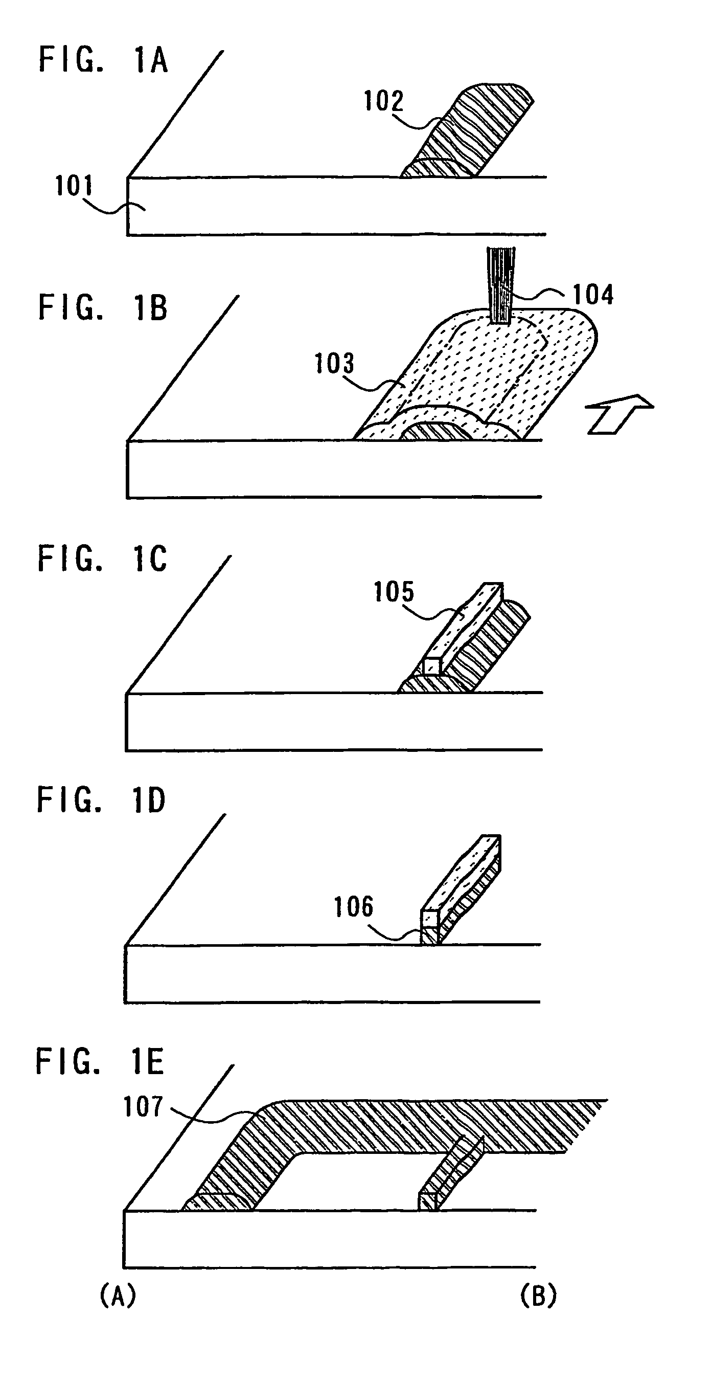
[0069]A step of forming a narrow wiring using a mask pattern formed by being irradiated with a laser beam (hereinafter, also referred to as laser light) is described in this embodiment mode with reference to FIGS. 1A to 1E and FIG. 2.
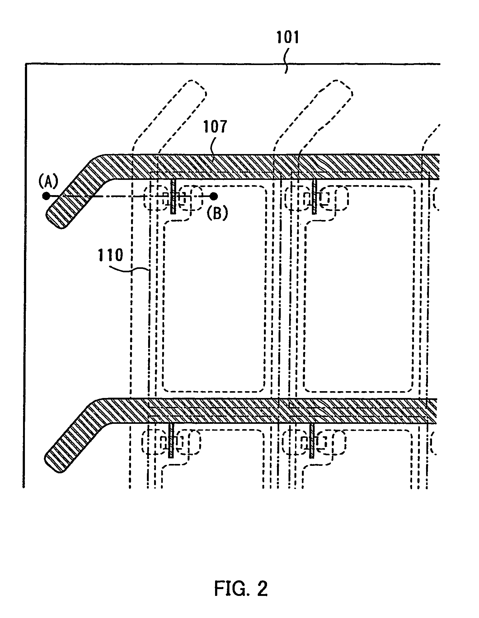
[0070]FIG. 2 is a plan view of a substrate 101 in which a pixel 110 is arranged in a matrix. A third conductive layer 107 which functions as a gate wiring of a semiconductor element to be formed later is shown in solid line over the substrate 101. In addition, a source wiring, a semiconductor region, a source electrode, a drain electrode, a pixel electrode, and the like of a semiconductor element to be formed later are shown in dashed line.
[0071]FIGS. 1A to 1E are front perspective views of the substrate in FIG. 2 taken along a line A-B. A manufacturing process of the invention is described with reference to FIGS. 1A to 1E.
[0072]A first conductive layer 102 is formed over the substrate 101 by a droplet discharge method as shown in FIG. 1A.
[0073]As the s...
embodiment mode 2
[0094]A method for manufacturing a semiconductor element is described hereinafter. The following embodiment mode is described using a TFT as a semiconductor element; however, the invention is not limited thereto. An organic semiconductor transistor, a diode, a MIM element, a memory element, a diode, a photoelectric conversion element, a capacitor element, a resistor element, or the like can be used.
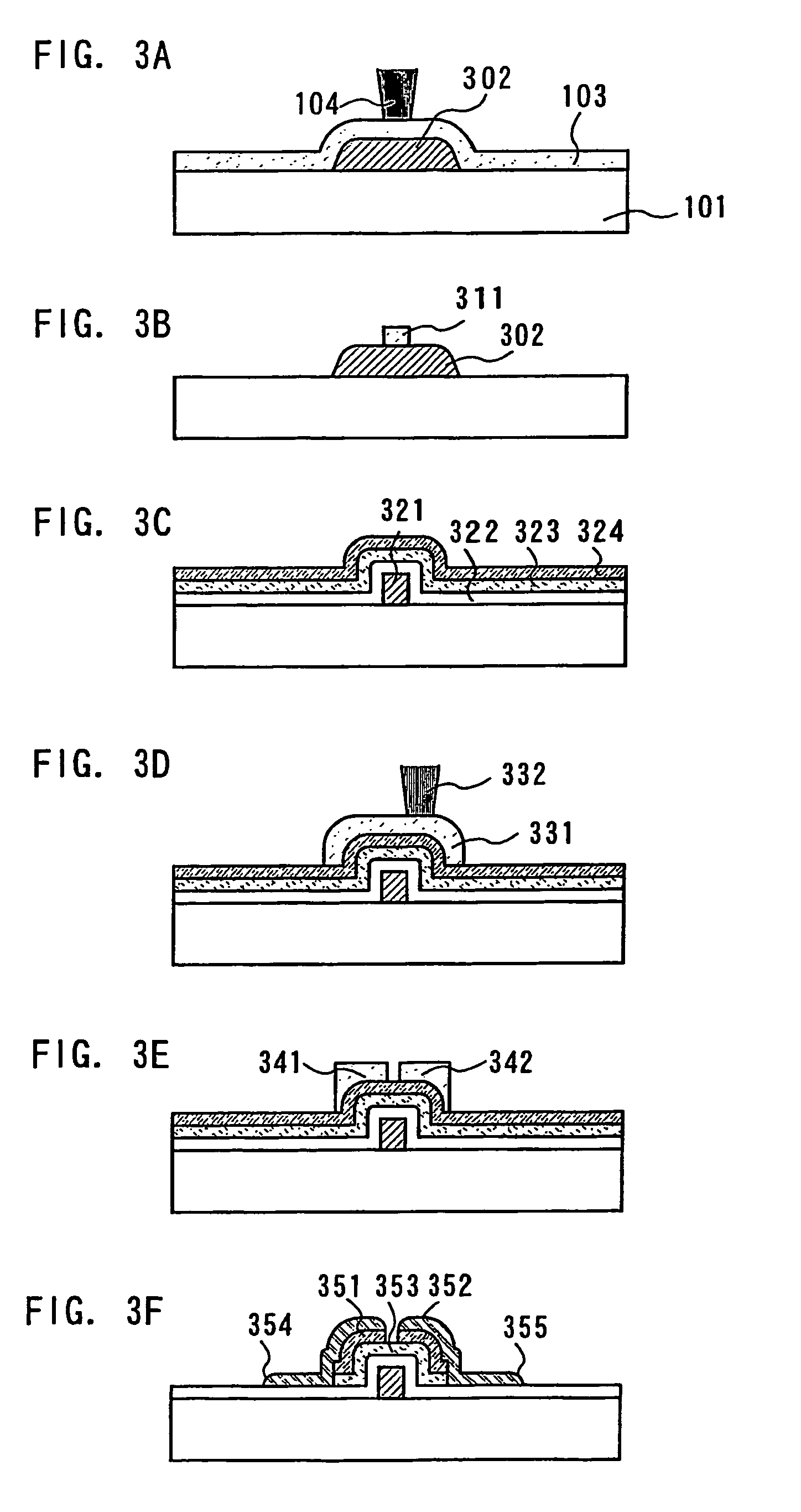
[0095]In this embodiment mode, a step of manufacturing a channel etch type TFT that is one of an inversely staggered type (bottom gate type) TFT as a semiconductor element is described with reference to FIGS. 3A to 3F.
[0096]As shown in FIG. 3A, a first conductive layer 302 is formed over a substrate 101. A droplet discharge method is employed as a formation method of the first conductive layer 302. In addition, the same conductive material as the first conductive layer 102 described in Embodiment Mode 1 can be appropriately used as a material of the first conductive layer.
[0097]Before the...
embodiment mode 3
[0116]A step of manufacturing a channel protective type (channel stopper type) TFT is described in this embodiment mode with reference to FIGS. 4A to 4E.
[0117]As in Embodiment Mode 2, after performing steps shown in FIGS. 4A and 4B, a gate electrode 321, a first insulating film 322, and a first semiconductor film 323 are formed over a substrate 101 as shown in FIG. 4C.
[0118]Subsequently, a protective film 401 is formed in a region over the first semiconductor film 323, which overlaps the gate electrode 321. The protective film is preferably formed by using a heat resistant high molecular weight material. It is preferable to use a high molecular weight material which has an aromatic ring or a heterocyclic ring as a main chain, has few aliphatic portions, and includes high polar heteroatom groups. As a typical example of such a high molecular weight material, polyimide, polybenzimidazole, or the like can be given. In the case of using polyimide, a composition containing polyimide is d...
PUM
| Property | Measurement | Unit |
|---|---|---|
| widths | aaaaa | aaaaa |
| viscosity | aaaaa | aaaaa |
| surface tension | aaaaa | aaaaa |
Abstract
Description
Claims
Application Information