Liquid crystal display device and alignment process method

Inactive Publication Date: 2008-02-21
FUJITSU LTD
View PDF12 Cites 2 Cited by
  • Summary
  • Abstract
  • Description
  • Claims
  • Application Information

AI Technical Summary

Benefits of technology

[0024] In the present invention, a region is provided that enables application of a voltage other than an output voltage from a driving unit, to a liquid crystal panel from the outside. Thus, for example, even when the alignment of the initial state is disarranged upon mounting a driving unit or upon assembling a module, by performing an alignment process by applying a voltage to the region, the alignment can be easily restored to its initial state with the driving unit being mounted. In addition, evaluation can be made such that the characteristics of the liquid crystal panel itself are distinguished from the characteristics of the driving unit. For example, when a display failure occurs, it is possible to determine which one of the liquid crystal panel and the driving unit is the cause of the failure.

Problems solved by technology

Hence, when moving image display (60 images / second) is performed on a liquid crystal display device using a TN liquid crystal, an image is blurred because liquid crystal molecules cannot fully operate, and thus, the TN liquid crystal is not suitable for use to perform multimedia moving image display.

Method used


Image

  • Liquid crystal display device and alignment process method
  • Liquid crystal display device and alignment process method
  • Liquid crystal display device and alignment process method

Examples


first embodiment

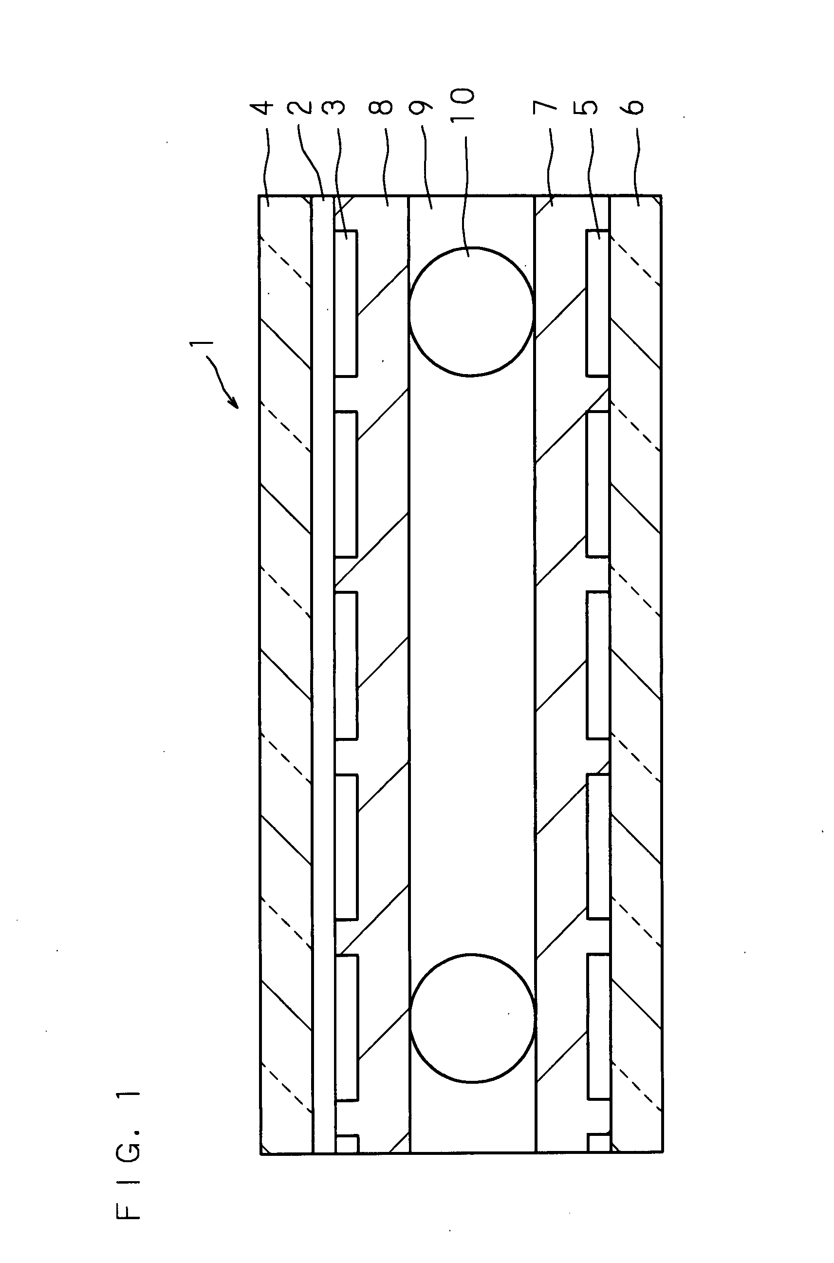
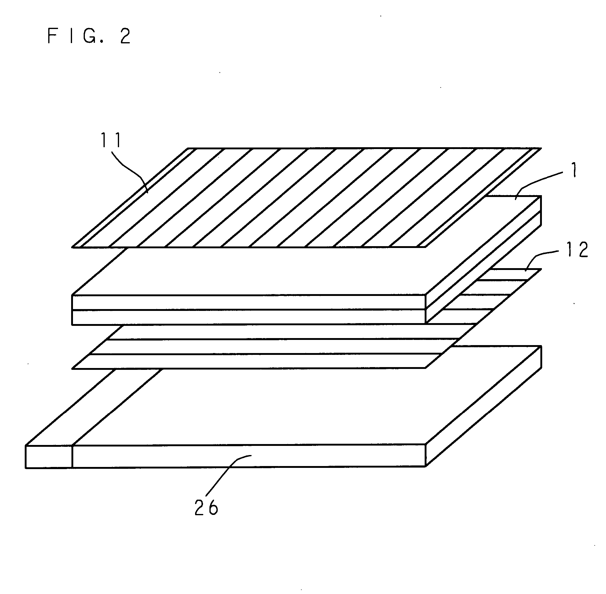
[0055]FIG. 1 is a schematic cross-sectional view showing a configuration of a liquid crystal panel. As shown in FIG. 1, a liquid crystal panel 1 includes a glass substrate 6 having pixel electrodes 5 (e.g., 0.08×0.24 mm2, number of pixels: 1024 H×3 RGB×768V, and 12.1-inch diagonal) composed of ITO (Indium Tin Oxide), disposed in a matrix form, and having an excellent light-transmitting property and TFTs connected to the pixel electrodes 5, respectively; and a glass substrate 4 having a counter electrode 2 and color filters 3 disposed in a matrix form.

[0056] An alignment film 7 and an alignment film 8 are provided on the pixel electrodes 5 and the color filters 3, respectively. The glass substrates 6 and 4 are disposed in such a manner that the alignment films 7 and 8 face each other. A liquid crystal layer 9 is formed by filling a ferroelectric liquid crystal into a space made by scattering, between the alignment films 7 and 8, spacers 10 (the shape is spherical, rectangular parall...

second embodiment

[0073] Since the configurations of the liquid crystal panel 1, the backlight 26, and their peripheral circuits according to a second embodiment are the same as those according to the first embodiment, the description thereof is omitted.

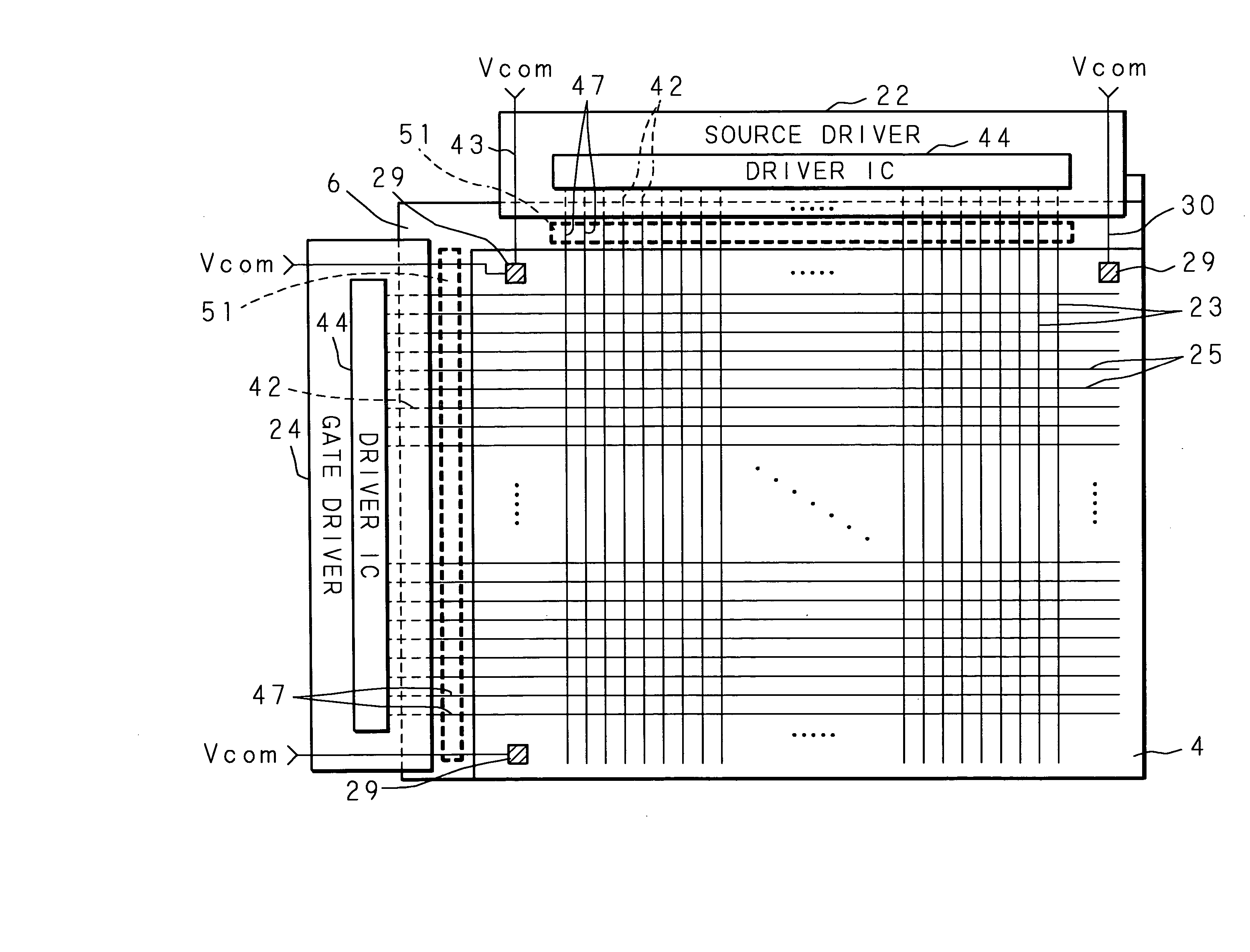
[0074] An alignment process of the second embodiment will be described. FIG. 6 is a diagram showing external voltage supply regions according to the second embodiment. In FIG. 6, the same parts as those in FIGS. 1 to 5 are denoted by the same reference numerals.

[0075] A region (a region surrounded by a dashed line in FIG. 6) where are put together all electrodes 47 which form part of the data lines 23 or the scan lines 25 connecting the driver IC 44 of the source driver 22 or the gate driver 24 which serves as a driving unit 40 to TFTs provided on the glass substrate 6, and which are on the side where the source driver 22 or the gate driver 24 is mounted, functions as an external voltage supply region 51 that receives, from the outside, application ...

third embodiment

[0079] Since the configurations of the liquid crystal panel 1, the backlight 26, and their peripheral circuits according to a third embodiment are the same as those according to the first embodiment, the description thereof is omitted.

[0080] An alignment process of the third embodiment will be described. FIG. 7 is a diagram showing external voltage supply regions according to the third embodiment. In FIG. 7, the same parts as those in FIGS. 1 to 5 are denoted by the same reference numerals.

[0081] A region (a region surrounded by a dashed line in FIG. 7) where are put together all electrodes 47 which form part of the data lines 23 or the scan lines 25 connecting the driver IC 44 of the source driver 22 or the gate driver 24 which serves as a driving unit 40 to TFTs provided on the glass substrate 6, and which are on the other side of the side where the source driver 22 or the gate driver 24 is mounted, functions as an external voltage supply region 61 that receives, from the outsid...


PUM


Abstract

Although portions of electrodes in proximity to a driver IC are covered with an insulating film, part of the electrodes is not covered with the insulating film. Thus, this insulating film absent region functions as an external voltage supply region that receives, from the outside, application of a voltage which is different from an output voltage from a driving unit. When the alignment of the initial state is disarranged, an alignment process is performed by short-circuiting all electrodes of the driving unit and applying a voltage from the outside, through the external voltage supply region, whereby the alignment is restored to the initial state with the driving unit being mounted on a liquid crystal panel.

Description

[0001] This application is a continuing application, filed under 35 U.S.C. §11(a), of International Application PCT / JP2005 / 007452, filed Apr. 19, 2005, the entire contents of which are incorporated herein by reference.TECHNICAL FIELD [0002] The present invention relates to a liquid crystal display device and an alignment process method. More particularly, the present invention relates to a liquid crystal display device having a region that receives application of a voltage from the outside, and an alignment process method of performing an alignment process for a liquid crystal material by a voltage application using the region. BACKGROUND ART [0003] A widespread used TN (Twisted Nematic) liquid crystal has a response speed of ten to several tens of milliseconds with respect to an applied voltage. The response speed suddenly becomes slow in halftone display having a different number of gradation levels and may reach a value close to one hundred milliseconds. Hence, when moving image ...

Claims


Application Information

Patent Timeline
IPC IPC(8): G09G3/36
CPCG02F1/133345G02F1/1345G02F1/13452G02F1/141G09G2300/0426G09G3/3651G09G3/3674G09G3/3685G09G3/2022G02F1/1337
Inventor MAKINO, TETSUYATADAKI, SHINJIYOSHIHARA, TOSHIAKISHIROTO, HIRONORIKIYOTA, YOSHINORIKASAHARA, SHIGEOBETSUI, KEIICHI
Owner FUJITSU LTD
Why Eureka
Try Eureka