Methods of forming semiconductor light emitting device packages by liquid injection molding and molded semiconductor light emitting device strips

a technology of semiconductor light emitting devices and liquid injection molding, which is applied in the field of semiconductor light emitting device packaging and packaging methods, can solve the problems of higher thermal impedance of such packages, complicated assembly, and higher reliability problems of packages, and achieve the effect of limiting the formation of air pockets

Active Publication Date: 2008-02-21
CREELED INC
View PDF37 Cites 59 Cited by
  • Summary
  • Abstract
  • Description
  • Claims
  • Application Information

AI Technical Summary

Benefits of technology

[0012]In further embodiments, liquid injection molding includes placing the substrate in a mold having a mold cavity having a shape that defines the optical element. Resin is injected into the mold. The injected resin is cured to form the optical element bonded to the substrate. The resin may be a thermoset resin and injecting the resin into the mold may be preceded by metering and mixing a hardener into the resin. Injecting the resin may include dispensing the resin into a receiving chamber of the mold and activating an injection plunger to move the resin from the receiving chamber into the mold cavity while removing substantially all air from the mold cavity to limit formation of air pockets in the optical element.

Problems solved by technology

As a result, the thermal impedance for such packages may be higher and a thermal mismatch may result among the various components within a package that may cause reliability problems with a package.
For example, problems may result at an interface between a copper metal of a heat sink or cavity with a plastic of a body in which such a heat sink or cavity is mounted.
In addition, assembly may be more complicated because of increased piece part counts for the package.
In addition, where a sheet metal optical cavity is utilized, a cavity typically can only be fabricated in a limited range of depth and shape configurations.
Such multipart packages may also have a larger optical cavity space, resulting in greater volumes of encapsulant being used, which may increase problems related to delamination and / or formation of bubbles within the encapsulant during temperature cycles.
Such a product may not be surface mount technology (SMT) compatible, as its packaging materials generally cannot withstand solder reflow temperatures.
In addition, during use, the soft encapsulant may tend to form bubbles or delaminate from the enclosure walls, which may adversely affect device reliability.
The use of a pre-molded lens attached by adhesive may encounter some problems in robustness and reliability of the finished product.
For example, the manufacturing process for such devices may be inherently inconsistent and the resultant package may be less robust and / or reliable.
However, epoxy tends to be degraded by the electromagnetic energy of blue light, generally generated by some semiconductor light emitting devices, and may become less transmissive to light as a result.
The resulting package may, therefore, become dimmer over a relatively short period of time.
As such, epoxy may be a less attractive option for encapsulating devices that emit blue light.
In addition, epoxy generally has a Coefficient of Thermal Expansion (CTE) mismatch problem with silicone soft gel, which may be used to junction coat the LED chips and their bond wires as the first layer of encapsulant.

Method used


Image

  • Methods of forming semiconductor light emitting device packages by liquid injection molding and molded semiconductor light emitting device strips
  • Methods of forming semiconductor light emitting device packages by liquid injection molding and molded semiconductor light emitting device strips
  • Methods of forming semiconductor light emitting device packages by liquid injection molding and molded semiconductor light emitting device strips

Examples


Embodiment Construction

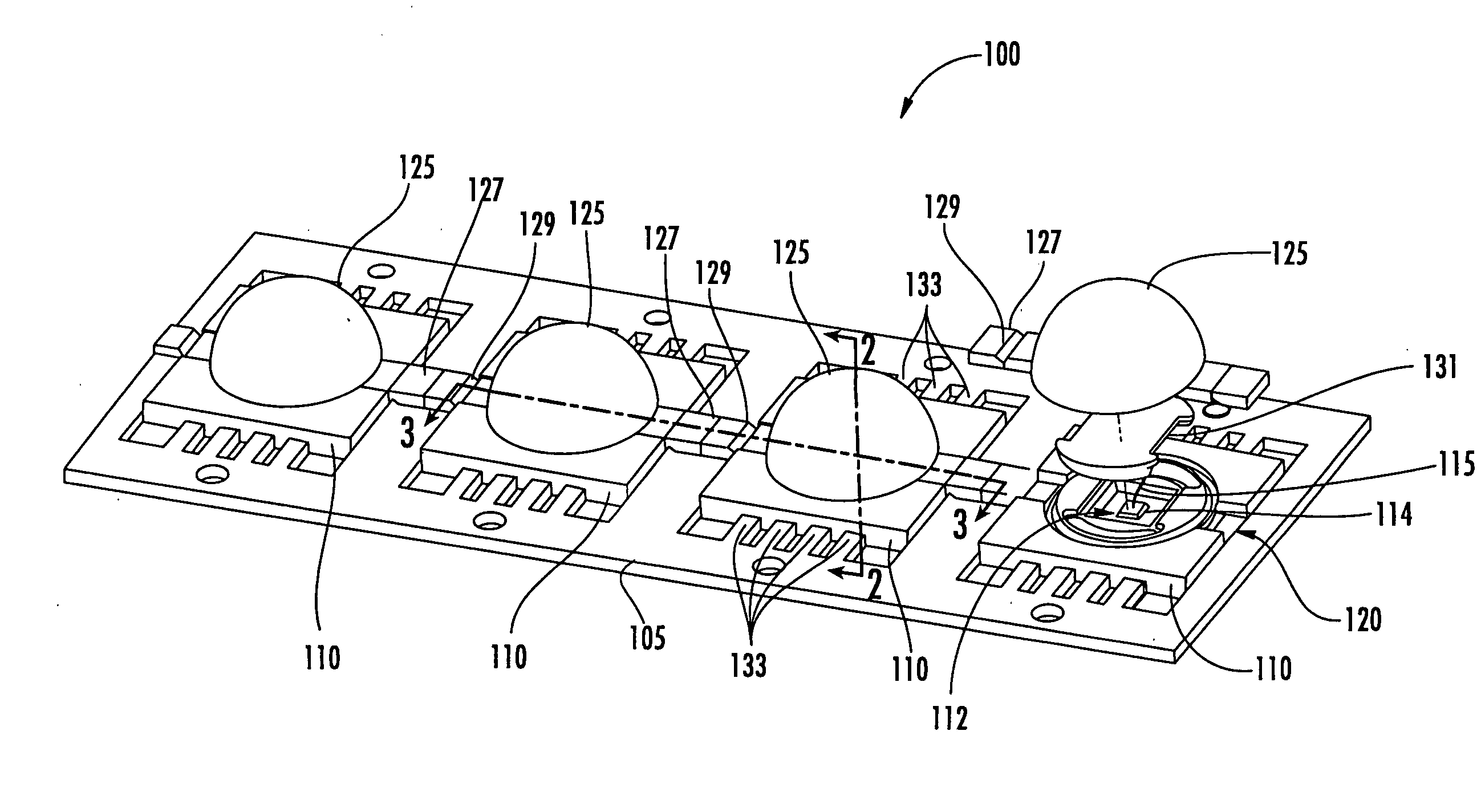
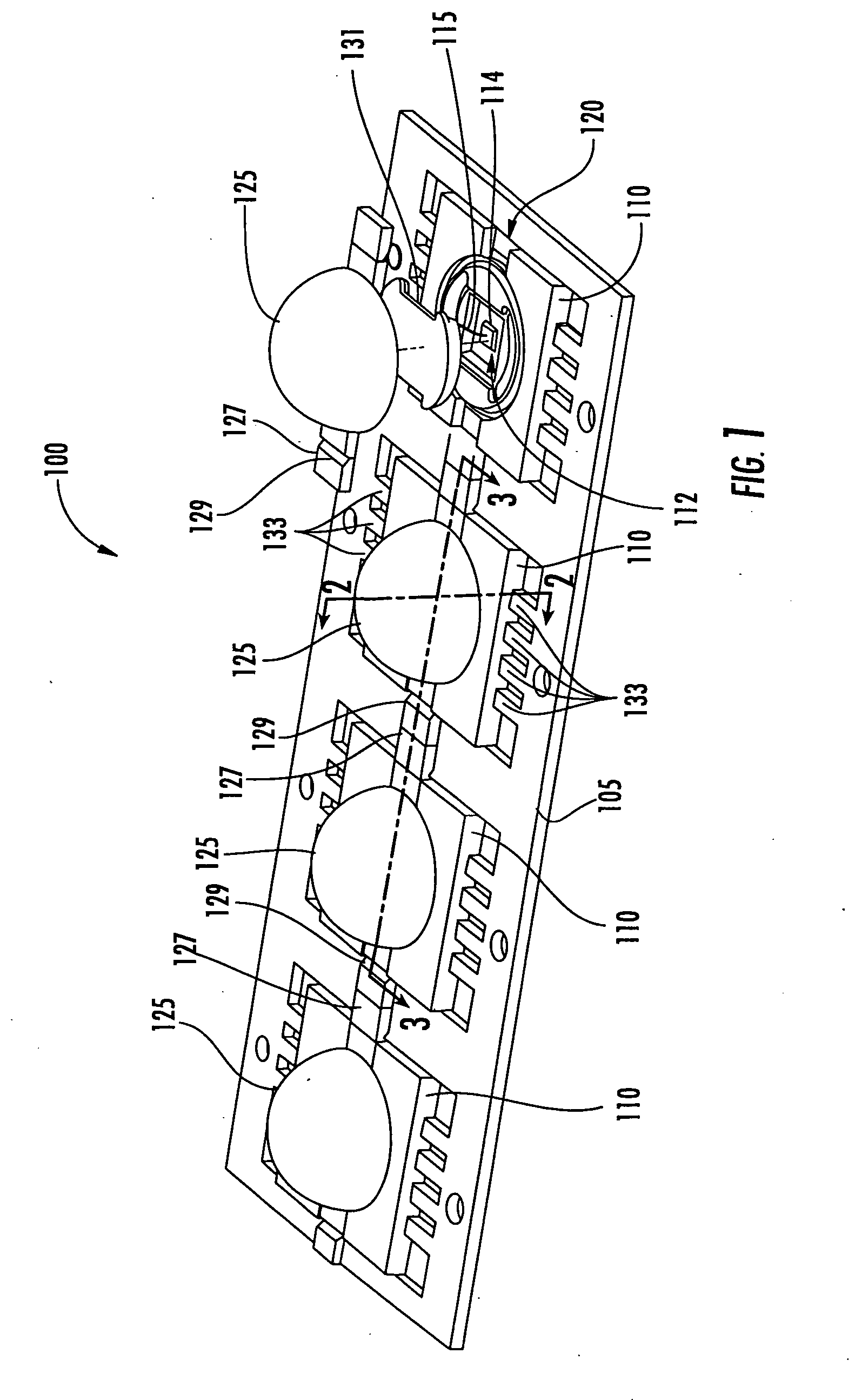
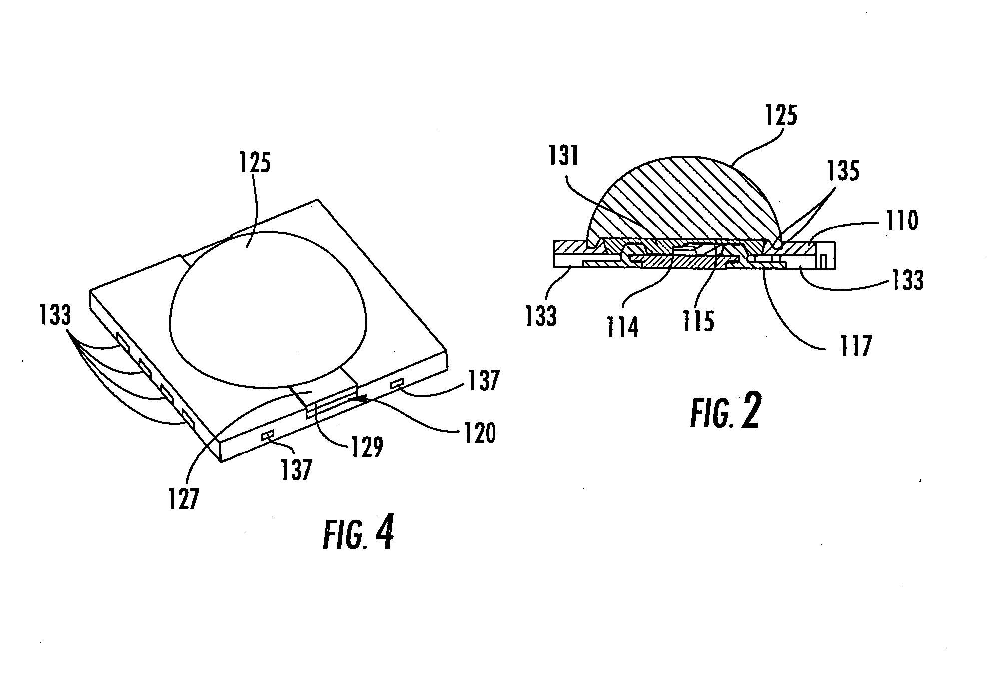
[0028]The invention is described more fully hereinafter with reference to the accompanying drawings, in which embodiments of the invention are shown. This invention may, however, be embodied in many different forms and should not be construed as limited to the embodiments set forth herein. Rather, these embodiments are provided so that this disclosure will be thorough and complete, and will fully convey the scope of the invention to those skilled in the art. In the drawings, the size and relative sizes of layers and regions may be exaggerated for clarity.

[0029]It will be understood that when an element or layer is referred to as being “on”, “connected to” or “coupled to” another element or layer, it can be directly on, connected or coupled to the other element or layer or intervening elements or layers may be present. In contrast, when an element is referred to as being “directly on,”“directly connected to” or “directly coupled to” another element or layer, there are no intervening ...


PUM

PropertyMeasurementUnit
pressureaaaaaaaaaa
pressureaaaaaaaaaa
mold temperatureaaaaaaaaaa

Abstract

Semiconductor light emitting device packaging methods include fabricating a substrate configured to mount a semiconductor light emitting device thereon. The substrate may include a cavity configured to mount the semiconductor light emitting device therein. The semiconductor light emitting device is mounted on the substrate and electrically connected to a contact portion of the substrate. The substrate is liquid injection molded to form an optical element bonded to the substrate over the semiconductor light emitting device. Liquid injection molding may be preceded by applying a soft resin on the electrically connected semiconductor light emitting device in the cavity. Semiconductor light emitting device substrate strips are also provided.

Description

BACKGROUND OF THE INVENTION[0001]This invention relates to semiconductor light emitting devices and manufacturing methods therefor, and more particularly to packaging and packaging methods for semiconductor light emitting devices.[0002]Semiconductor light emitting devices, such as Light Emitting Diodes (LEDs) or laser diodes, are widely used for many applications. As is well known to those having skill in the art, a semiconductor light emitting device includes one or more semiconductor layers that are configured to emit coherent and / or incoherent light upon energization thereof. It is also known that the semiconductor light emitting device generally is packaged to provide external electrical connections, heat sinking, lenses or waveguides, environmental protection and / or other functions.[0003]For example, it is known to provide a two-piece package for a semiconductor light emitting device, wherein the semiconductor light emitting device is mounted on a substrate that comprises alumi...

Claims


Application Information

Patent Timeline
Patent Type & Authority Applications(United States)
IPC IPC(8): H01L21/00H01L33/52H01L33/58
CPCB29C45/14655B29C45/14836H01L2924/12041H01L2224/48247H01L2224/48091B29C45/34B29C2045/14844B29K2083/00B29K2995/0018B29L2011/0016H01L33/52H01L33/58H01L24/97H01L2924/00014H01L2924/00H01L2924/181
Inventor LOH, BAN P.MEDENDORP, NICHOLAS W.
Owner CREELED INC
Why Eureka
Try Eureka