Metal core foldover package structures, systems including same and methods of fabrication

a technology of metal core and package structure, applied in the field of chipscale packages, can solve the problems of large distance of protruding vsmps above the carrier substrate, many vsmp designs are somewhat costly to implement, and require fairly complex and sophisticated carrier substrates

Active Publication Date: 2008-02-28
MICRON TECH INC
View PDF27 Cites 113 Cited by
  • Summary
  • Abstract
  • Description
  • Claims
  • Application Information

AI Technical Summary

Problems solved by technology

However, many VSMP designs are somewhat costly to implement and require fairly complex and sophisticated carrier substrates.
In addition, for some applications, the relatively large distance of protrusion of the VSMPs above the carrier substrate is unaccept...

Method used


Image

  • Metal core foldover package structures, systems including same and methods of fabrication
  • Metal core foldover package structures, systems including same and methods of fabrication
  • Metal core foldover package structures, systems including same and methods of fabrication

Examples


Embodiment Construction

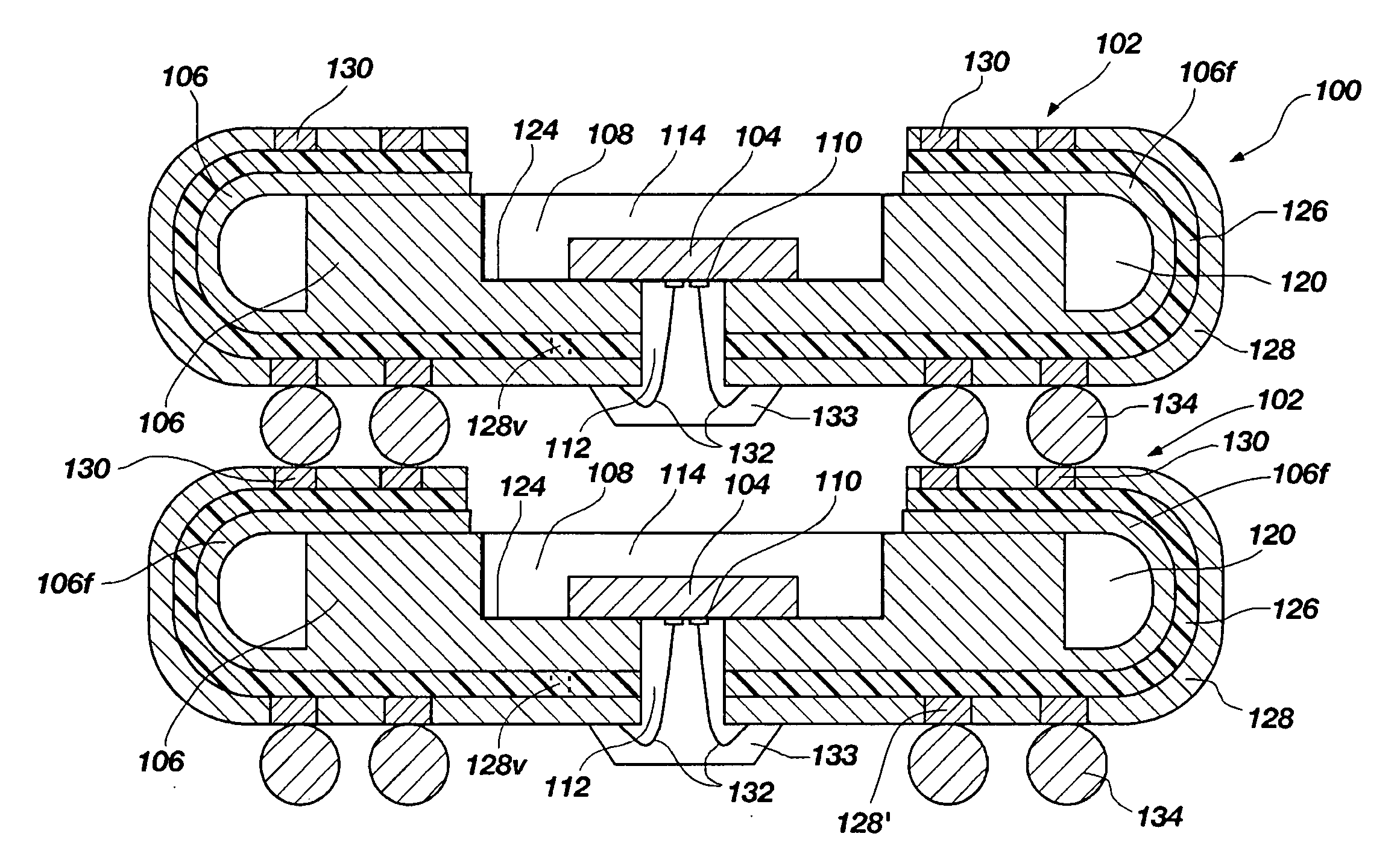
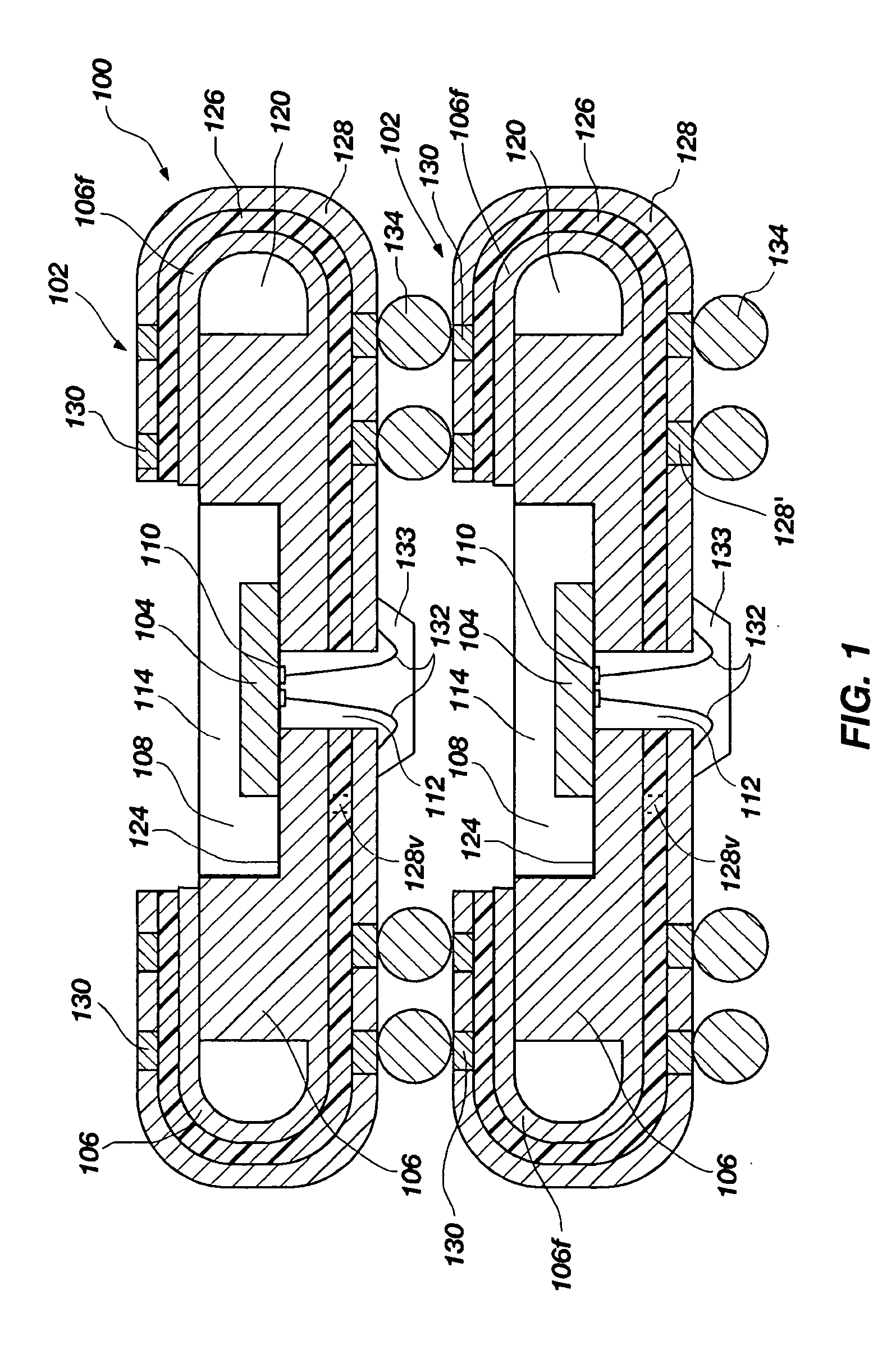
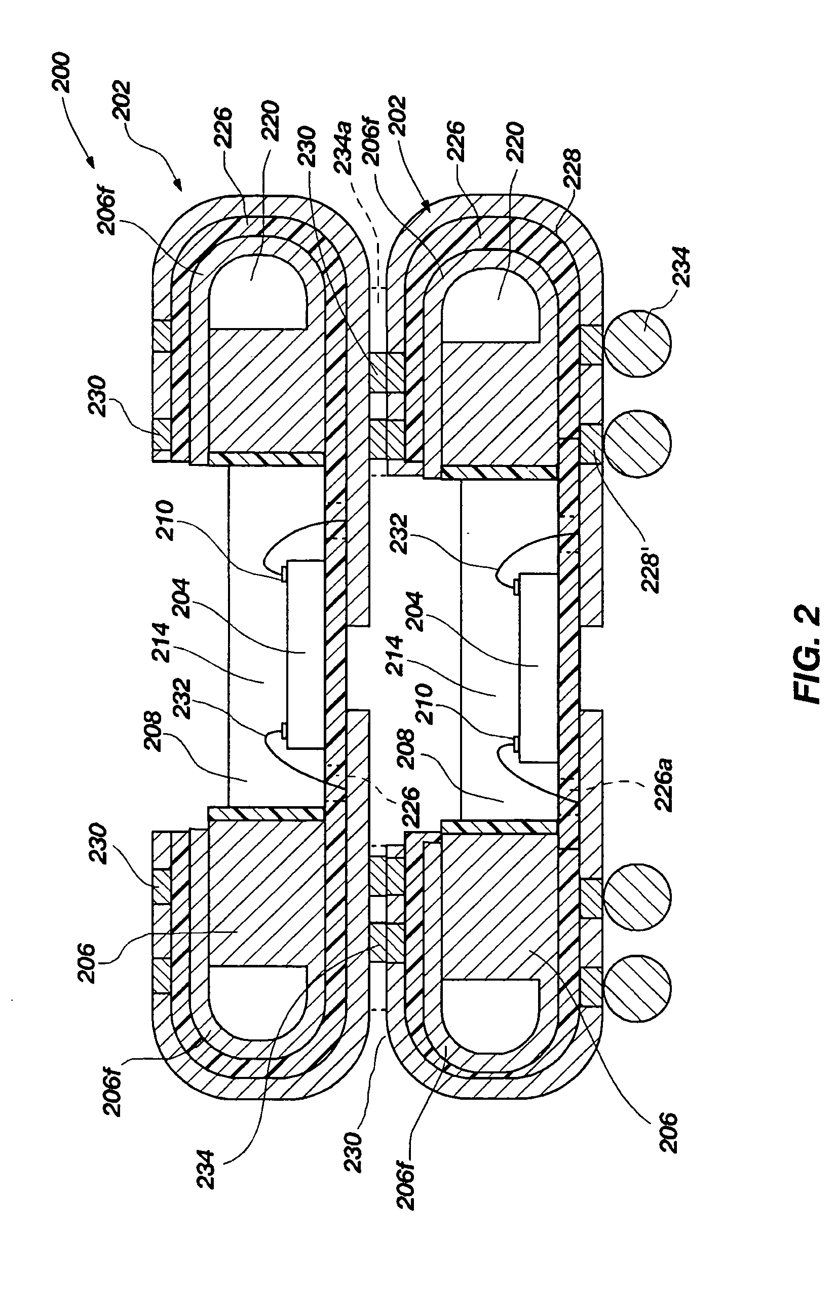
[0015]Embodiments of chip scale packages are disclosed, as well as to embodiments of methods of fabricating such packages including, by way of example only, Chip-On-Board (COB) and Board-On-Chip (BOC) packages. Also disclosed are embodiments of vertically stacked Package-On-Package (POP) modules, and systems including COB and BOC packages and POP modules.

[0016]Embodiments of the chip scale package may include a core member formed from a metal or metal alloy and having at least one portion partially folded over itself. These embodiments provide a minimized footprint, substantially chip scale package of robust design exhibiting enhanced rigidity that provides a capability of stacking multiple semiconductor dice. Such embodiments also provide a capability to convert semiconductor dice exhibiting a peripheral or central bond pad I / O arrangement into array-type chip scale packages. Yet a further advantage of the various embodiments of chip scale packages of the present invention is impro...


PUM

PropertyMeasurementUnit
Thicknessaaaaaaaaaa
Dielectric polarization enthalpyaaaaaaaaaa
Massaaaaaaaaaa

Abstract

Chip scale packages and assemblies thereof and methods of fabricating such packages including Chip-On-Board, Board-On-Chip, and vertically stacked Package-On-Package modules are disclosed. The chip scale package includes a core member of a metal or alloy having a recess for at least partially receiving a die therein and includes at least one flange member partially folded over another portion of the core member. Conductive traces extend from one side of the package over the at least one flange member to an opposing side of the package. Systems including the chip scale packages and assemblies are also disclosed.

Description

BACKGROUND OF THE INVENTION[0001]1. Field of the Invention[0002]Embodiments of the invention relate to chip-scale packages (CSPs), stacking integrated such CSPs in a multi-chip module (MCM) structure in a package-on-package (POP) configuration, and methods of forming such packages and structures.[0003]2. Discussion of Related Art[0004]Semiconductor dice are conventionally packaged individually in transfer-molded resin packages or, less commonly, ceramic packages. Packaging supports, protects, and (in some instances) dissipates heat from the semiconductor die and provides a lead system for power and ground or bias as well as signal distribution to and from the semiconductor die or dice within. The die package may also facilitate burn-in and other testing of each semiconductor die or dice in the package prior to and after its assembly with higher level packaging.[0005]One type of integrated circuit (IC) or semiconductor die package is referred to as a “chip scale package,”“chip size p...

Claims


Application Information

Patent Timeline
IPC IPC(8): H01L23/02H01L21/00
CPCH01L23/13Y10T29/49124H01L23/36H01L23/3735H01L23/5387H01L25/105H01L2224/48091H01L2224/48227H01L2224/4824H01L2924/01078H01L2924/09701H01L2924/14H01L2924/15311H01L2924/3025H01L23/3128H01L2224/73215H01L2224/32225H01L2225/1058H01L2225/1041H01L2924/01087H01L2924/01019H01L24/48H01L2924/00014H01L2924/00012H01L2924/00H01L2924/181H01L2924/15153B33Y80/00H01L2224/45099H01L2224/45015H01L2924/207H01L23/02
Inventor CORISIS, DAVID J.CHONG, CHIN HUILEE, CHOON KUAN
Owner MICRON TECH INC
Why Eureka
Try Eureka