Display device and manufacturing method thereof

a technology of display device and manufacturing method, which is applied in the manufacture of semiconductor devices, semiconductor/solid-state device details, electric discharge tube/lamps, etc., can solve the problems of limited thickness reduction, difficult to reduce the thickness of sealing mother substrate and tft mother substrate equal or more than cutting allowable thicknesses, etc., to facilitate the reduction of thickness and weight of display device, reduce the number of steps, and reduce the effect of cos

Active Publication Date: 2008-02-28
SAMSUNG DISPLAY CO LTD +1
View PDF1 Cites 4 Cited by
  • Summary
  • Abstract
  • Description
  • Claims
  • Application Information

AI Technical Summary

Benefits of technology

[0011]According to the present invention, it is possible to facilitate the reduction of thickness and the reduction of weight of a display device and, at the same time, to reduce the number of steps and to reduce a cost by simultaneously performing etching and cutting.
[0012]Further, it is possible to eliminate the restriction imposed on cutting of a thin plate which has been a drawback at the time of cutting out display devices from a large-sized mother substrate thus realizing the mass production of thinner display devices.

Problems solved by technology

However, the reduction of thickness is limited due to the restriction imposed on a production process.
In such a cutting step, the thicknesses of the TFT mother substrate and the sealing mother substrate which enable cutting of these mother substrates are limited and hence, in the etching step which is a preceding step of the cutting step, currently, it is difficult to reduce the thicknesses of the sealing mother substrate and the TFT mother substrate equal to or more than the cutting allowable thicknesses.

Method used


Image

  • Display device and manufacturing method thereof
  • Display device and manufacturing method thereof
  • Display device and manufacturing method thereof

Examples


embodiment 1

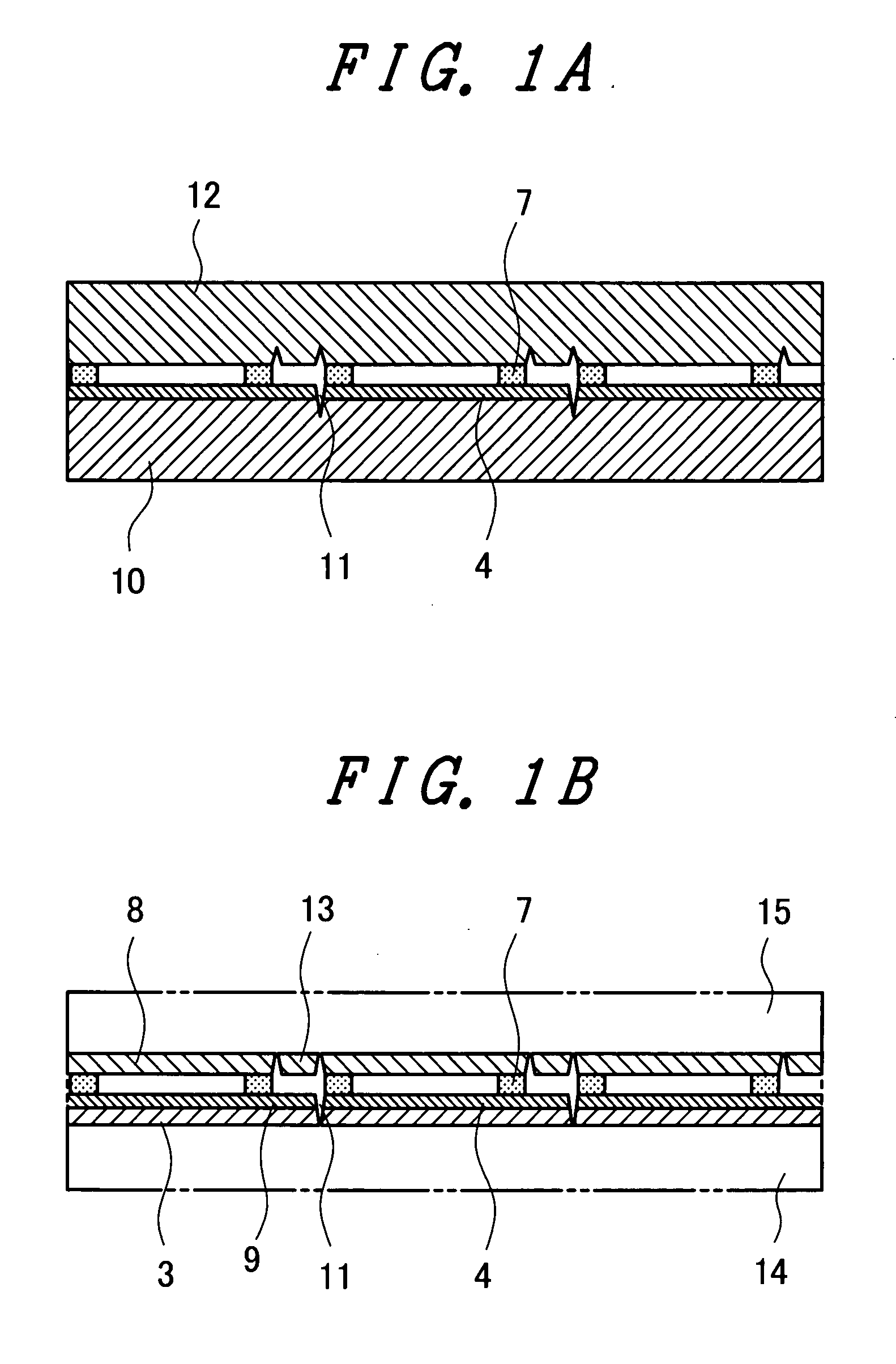
[0022]FIG. 1A and FIG. 1B are cross-sectional views of mother substrates on which a plurality of display devices is formed, wherein FIG. 1A shows the mother substrates before etching and FIG. 1B shows the mother substrates after etching.

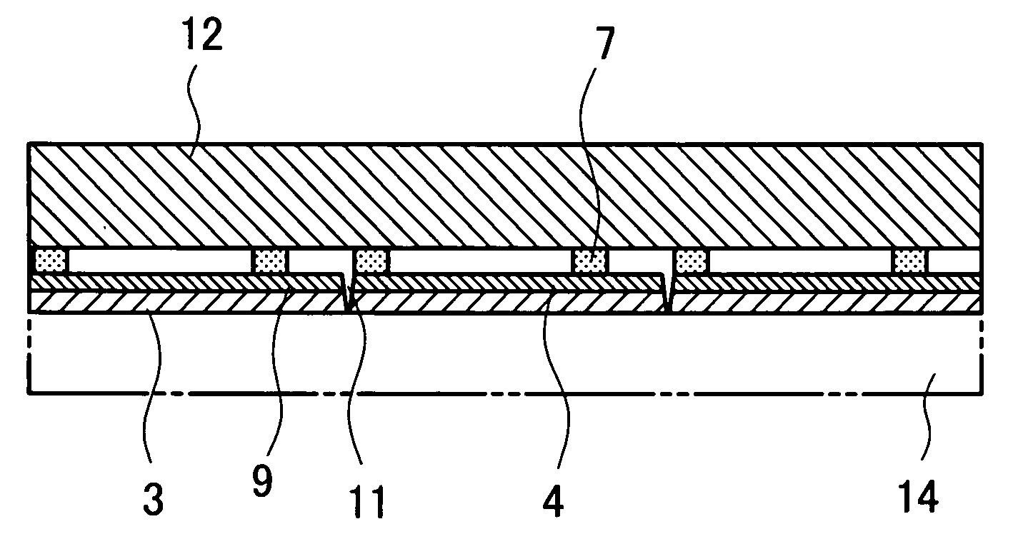
[0023]In FIG. 1A, to a TFT mother substrate 10 on which thin film transistor (TFT) circuit layers 4 which drive organic ELs, liquid crystal and the like as display elements are formed, a sealing mother substrate 12 is adhered in an opposedly facing manner using an adhesive layer 7. On back surfaces of the TFT mother substrate 10 and the sealing mother substrate 12, scribe marks 11 for separating the TFT mother substrate 10 and the sealing mother substrate 12 into a plurality of display devices are preliminarily formed. These substrates are made of alkali-free glass.

[0024]In FIG. 1B, front surfaces of the TFT mother substrate 10 and the sealing mother substrate 12 are etched, and etching portions 14, 15 reach the scribe marks 11 and hence, the individ...

embodiment 2

[0032]FIG. 7 is a cross-sectional view of the mother substrate when only the TFT mother substrate is etched. FIG. 8 is a cross-sectional view of the mother substrate when only the sealing mother substrate is etched.

[0033]In FIG. 7, when only the TFT mother substrate is etched as indicated by the etching portion 14, the sealing mother substrate 12 is mechanically broken. In this case, as shown in FIG. 1A, the scribe marks may be preliminarily formed on the back surface of the sealing mother substrate 12 or the scribe marks may be formed on the front surface of the sealing mother substrate 12.

[0034]In FIG. 8, when only the sealing mother substrate is etched as indicated by the etching portion 15, the TFT mother substrate 10 is mechanically broken in the same manner. In this case, as shown in FIG. 1A, the scribe marks may be preliminarily formed on the back surface of the TFT mother substrate 10 or the scribe marks may be formed on the front surface of the TFT mother substrate 10.


PUM


Abstract

The present invention provides a manufacturing method of a display device which can efficiently separate individual thin-thickness display devices from a large-sized mother substrate. Scribe marks for separating a plurality of display devices are preliminarily formed on back surfaces of a TFT mother substrate and a sealing mother substrate. By etching front surfaces of these mother substrates, etching portions reach the scribe marks so that a plurality of display devices each of which is constituted of a TFT substrate and a sealing substrate can be separated from each other.

Description

CROSS-REFERENCE TO RELATED APPLICATIONS[0001]The disclosure of Japanese Patent Application No. P2006-228981 filed on 2006 / 08 / 25 (yyyy / mm / dd) including the claims, the specification, the drawings and the abstract is incorporated herein by reference in its entirety.BACKGROUND[0002]1. Field of the Invention[0003]The present invention relates to a display device which is separated from a large-sized mother substrate on which a plurality of display devices is formed and a manufacturing method which manufactures individual display devices by separating these display devices.[0004]2. Description of the Related Art[0005]With respect to various display devices, particularly, an organic EL display device is extremely advantageous due to self-luminous light thereof and can facilitate the reduction of thickness and the reduction of weight of the display device. However, the reduction of thickness is limited due to the restriction imposed on a production process.[0006]Under a current manufacturi...

Claims


Application Information

Patent Timeline
Patent Type & Authority Applications(United States)
IPC IPC(8): H01J9/24H01L27/15
CPCH01L51/56H01L51/5237H10K50/841H10K50/8426H10K71/00
Inventor AZUMA, HITOSHITANAKA, MASAHIROMATSUURA, TOSHIYUKI
Owner SAMSUNG DISPLAY CO LTD
Why Eureka
Try Eureka