Process and temperature-independent voltage controlled attenuator and method

a voltage control and attenuator technology, applied in the direction of amplification control device circuits, pulse automatic control, electrical apparatus, etc., can solve the problems of degrading the quality of displayed images, image artifacts caused by lack of precise channel matching, and achieving only +1 db gain precision, etc., to achieve high precision

Active Publication Date: 2008-02-28
TEXAS INSTR INC
View PDF23 Cites 20 Cited by
  • Summary
  • Abstract
  • Description
  • Claims
  • Application Information

AI Technical Summary

Benefits of technology

[0011]It is an object of the invention to provide a high precision, voltage-controlled (or current-controlled) variable gain circuit element which can be utilized to provide ripple-free control of attenuation, gain, or other circuit or system parameters without resorting to piecewise-linear approximation techniques.
[0012]It is another object of the invention to provide a high precision, voltage-controlled (or current-controlled) variable gain circuit element which can be utilized to provide ripple-free control of attenuation, gain, or other circuit or system parameters without resorting to piecewise-linear approximation techniques, and which is substantially independent of the effects of integrated circuit process parameter variations and / or temperature variations.
[0021]In one embodiment, the invention provides a method for precision control of a variable resistor, including providing a first variable resistor (13) having a first terminal and a second terminal, and also having a resistance control terminal (16), a resistance between the first terminal and the second terminal being variable in response to a resistance control signal (VADJ) on the resistance control terminal. The method includes supplying a first current (I1) through a first conductor (14) to a first terminal of a reference resistor (11) having a second terminal connected to a reference voltage conductor (GND), supplying a second current (I2) through a second conductor (15) to the first terminal of the first variable resistor (13), and forcing a resistance of the first variable resistor (13) to be equal to a resistance of the first resistor (11) by sensing and amplifying a voltage difference between the first (14) and second (15) conductors to produce the first resistance control signal (VADJ) so as to minimize the voltage difference between the first (14) and second (15) conductors, to thereby cause the first variable resistor (13) to have the same precision as the reference resistor (11).
[0022]In one embodiment, the invention provides a circuit including a first variable resistor (13) having a first terminal and a second terminal, and also having a resistance control terminal (16), a resistance between the first terminal and the second terminal being variable in response to a resistance control signal (VADJ) on the resistance control terminal. The circuit means for supplying a first current (I1) through a first conductor (14) to a first terminal of a reference resistor (11) having a second terminal connected to a reference voltage conductor (GND), and also includes means for supplying a second current (I2) through a second conductor (15) to the first terminal of the first variable resistor (13), and means for forcing a resistance of the first variable resistor (13) to be equal to a resistance of the first resistor (11) by sensing and amplifying a voltage difference between the first (14) and second (15) conductors to produce the resistance control signal (VADJ) so as to minimize the voltage difference between the first (14) and second (15) conductors, to thereby cause the first variable resistor (13) to have the same precision as the reference resistor (11).

Problems solved by technology

This is desirable because the lack of precise channel matching creates image “artifacts” which have the effect of degrading the quality of the displayed image.
In effect, the image artifacts caused by the lack of precise channel matching may be erroneously interpreted as meaningful signals by an image processor.
Unfortunately, one of the most unpredictable elements in this signal processing progression is the voltage controlled variable gain amplifier.
This technique achieves only +−1 dB gain precision, and typically is complex and costly.
However, the precision of the resistance of FET resistors is very poor.

Method used


Image

  • Process and temperature-independent voltage controlled attenuator and method
  • Process and temperature-independent voltage controlled attenuator and method
  • Process and temperature-independent voltage controlled attenuator and method

Examples


Embodiment Construction

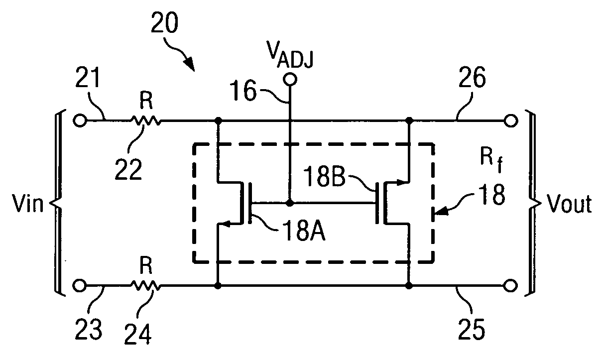
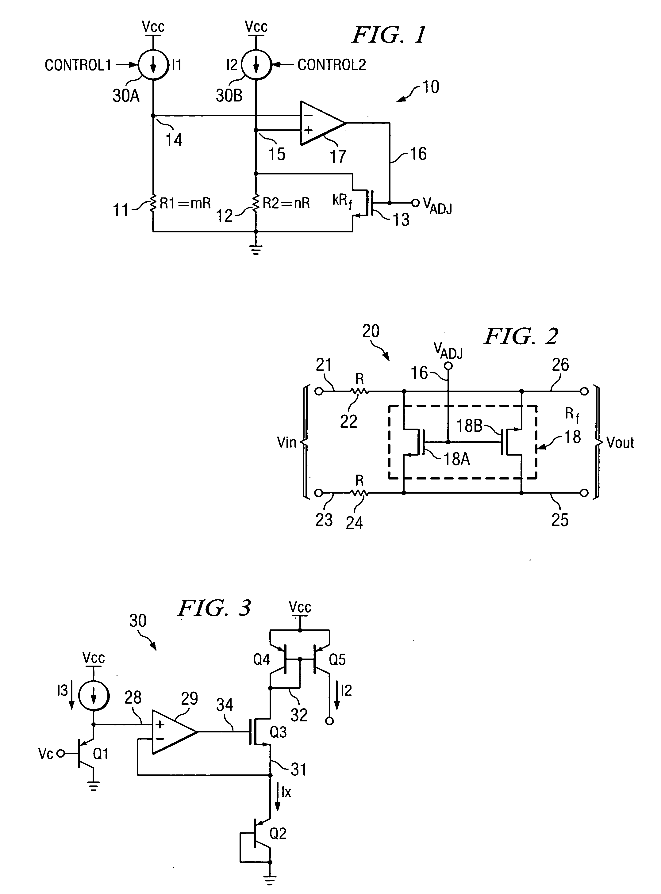
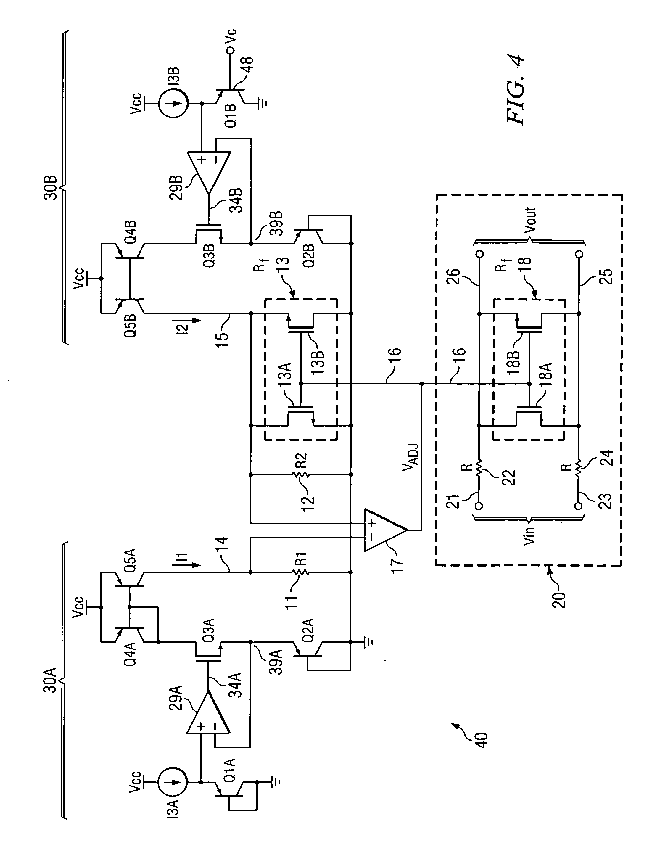
[0031]The present invention provides a technique and architecture that provide a new way to create a very accurate voltage-controlled resistor which may be used to control, for example, the attenuation in dB of an attenuator or the gain in dB of a variable gain amplifier. Instead of the gain being created by a piece-wise approximation to an ideal gain curve as in the above described prior art, the gain curve in accordance with one embodiment of the present invention depends upon a mathematical formula that is almost independent of integrated circuit manufacturing process variations and temperature variations.

[0032]The structure and technique of the invention are based upon “slaving” a relatively inaccurate voltage controlled resistor to a precision reference resistor in order to cause the voltage controlled resistor to have the same precision as the reference resistor. In one embodiment of the invention, the voltage controlled resistor is implemented as a FET (field effect transisto...


PUM


Abstract

A circuit includes a first variable resistor having a resistance which is variable in response to a resistance control signal. A resistance control circuit includes a first current source circuit for supplying a first current through a reference resistor. A second current source circuit supplies a second current through the first variable resistor. In operational amplifier has a first input coupled to a first conductor connecting the first current source to the reference resistor, a second input coupled to a second conductor connecting the current source to the first variable resistor, and an output applying the first resistance control signal to a control terminal of the first variable resistor, to force the resistance of the first variable resistor to be equal to a resistance of the reference resistor. The resistance of a second variable resistor of an attenuator is controlled in response to the resistance control signal.

Description

BACKGROUND OF THE INVENTION[0001]The present invention relates generally to voltage controlled variable gain attenuators and amplifiers, and more particularly to a voltage controlled variable gain attenuator and amplifier having a gain curve that is nearly independent of the effects of process variation and temperature variation.[0002]Present medical ultrasound and industrial imaging systems employ as many as 256 signal processing channels to create a clear image. Advances in the technology associated with signal processing in this area indicate that the channel count may be higher in future systems. A typical ultrasound channel consists of a piezo-electric transducer that supplies a signal to a variable gain amplifier which in turn drives an analog to digital converter. The piezo-electric transducer is excited by a high voltage transmitter which creates a signal that is applied (for example) to a patient or to industrial material undergoing an imaging examination. The output of the...

Claims


Application Information

Patent Timeline
Patent Type & Authority Applications(United States)
IPC IPC(8): H03L5/00
CPCH03G1/007
Inventor KOEN, MYRON J.
Owner TEXAS INSTR INC
Why Eureka
Try Eureka