

Coupled lamb wave resonators filter
- Summary
- Abstract
- Description
- Claims
- Application Information
AI Technical Summary
Benefits of technology
Problems solved by technology
Method used
Image

Examples
first embodiment
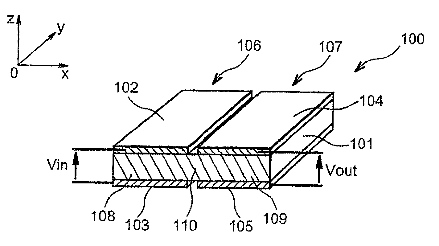
[0033]Referring first to FIG. 1, a coupled Lamb wave resonator filter 100 is shown. In the following description, the coupled Lamb wave resonator filter 100 is described without a periodic lattice between its resonators.
[0034]The coupled Lamb wave resonator filter 100 comprises a resonant layer 101 that may be based on a piezoelectric material such as aluminium nitride and / or zinc oxide or even PZT. Two electrodes 102 and 104 are arranged adjacent to each other on the resonant layer 101. In FIG. 1, these two electrodes 102 and 104 are separated from each other. Two other electrodes 103 and 105 are arranged adjacent to each other under the resonant layer 101. These other two electrodes 103 and 105 are also separated from each other. In FIG. 1, all electrodes 102 to 105 have the same length and are aligned vertically in pairs, and can be made conventionally, for example based on platinum, aluminium, molybdenum and / or tungsten.
[0035]A part 108 of the resonant layer 101 located between...
second embodiment
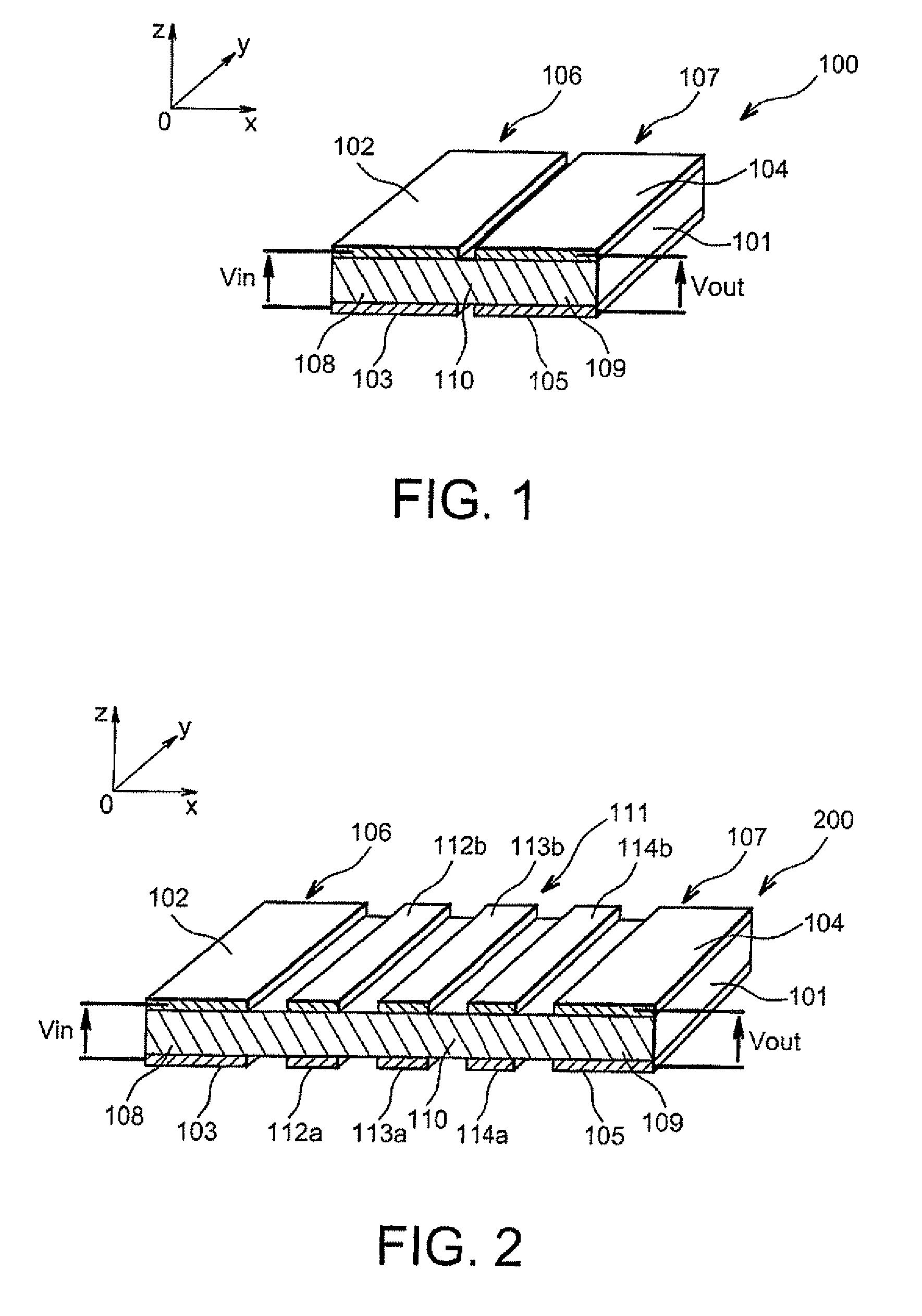
[0046]In this second embodiment, the coupled Lamb wave resonators filter 200 is made to obtain a narrow passband at the output centered around a central frequency equal to about
fc=cλc.
In this case, the length of the layer of resonant material 101 is equal to about
[0047]11λc4.
As in the first embodiment, the length of each resonator 106, 107 is about
[0048]λc2.
Therefore, in this case the length of the portion of resonant material 110 of the periodic lattice 111 is equal to about
[0049]7λc4.
[0050]The periodic lattice 111 comprises a first pair of metal areas 112a, 112b arranged above and below the portion of resonant material 110, and are vertically aligned with each other. These metal areas 112a, 112b are arranged at a distance of about
λc4
from the first resonator 106. A second pair of metal areas 113a, 113b, similar to the first pair of metal areas 112a, 112b, is arranged at a distance of about
λc4
from the first pair of metal areas 112a, 112b. Finally, a third pair of metal areas 114a, 1...
third embodiment
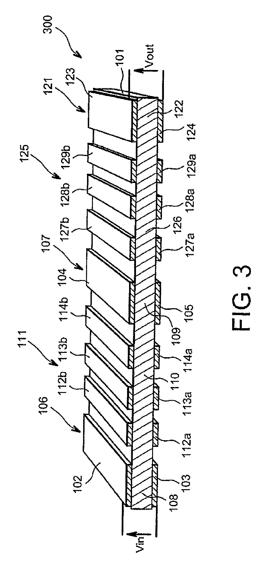
[0059]It is also possible to use periodic lattices to acoustically couple more than two resonators. FIG. 3 shows a coupled Lamb wave resonator 300 according to a
[0060]This filter 300 comprises a first Lamb wave resonator 106 coupled to a second Lamb wave resonator 107 by a first periodic lattice 111. These three elements may be similar to the elements shown in FIG. 2. The filter 300 also comprises a third Lamb wave resonator 121 comprising a resonant layer 122 arranged between two electrodes 123, 124 in a manner similar to the two other resonators 106, 107. The second and third resonators 107 and 121 are acoustically coupled through a second periodic lattice 125, for example similar to the first periodic lattice 111. The second periodic lattice 125 comprises a layer of resonant material 126 arranged between a plurality of pairs of metal areas 127 to 129 arranged on the layer 126 in a manner similar to the metal areas 112 to 114 on the layer 110.
[0061]In this embodiment, the layers 1...
PUM
| Property | Measurement | Unit |
|---|---|---|
| Time | aaaaa | aaaaa |
| Length | aaaaa | aaaaa |
| Distance | aaaaa | aaaaa |
Abstract
Description
Claims
Application Information