Method for producing substrate assembly for plasma display panel, and plasma display panel

a technology of plasma display panel and substrate, which is applied in the manufacture of electrode systems, electric discharge tubes/lamps, instruments, etc., can solve the problems of uneven evaporated dispersion medium, inability to form evenly the magnesium oxide crystal layer,

Inactive Publication Date: 2008-02-28
FUJITSU HITACHI PLASMA DISPLAY LTD
View PDF0 Cites 36 Cited by
  • Summary
  • Abstract
  • Description
  • Claims
  • Application Information

AI Technical Summary

Benefits of technology

[0014]According to the invention, when the suspension containing the magnesium oxide crystals is applied to the dielectric layer surface, the magnesium oxide crystals are trapped in the rugged surface structure formed uniformly in the dielectric layer surface and the dispersion medium of the suspension is evaporated in such a state, so that a layer of the magnesium oxide crystals can be evenly formed. Accordingly, a problem that the magnesium oxide crystals are agglomerated or that the dispersion medium is unevenly evaporated will not be caused.

Problems solved by technology

However according to this method, the layer of the magnesium oxide crystals sometimes cannot be formed evenly, because, at the time of evaporation of the dispersion medium, the magnesium oxide crystals can be agglomerated or the dispersion medium can be unevenly evaporated.
Accordingly, a problem that the magnesium oxide crystals are agglomerated or that the dispersion medium is unevenly evaporated will not be caused.

Method used


Image

  • Method for producing substrate assembly for plasma display panel, and plasma display panel
  • Method for producing substrate assembly for plasma display panel, and plasma display panel
  • Method for producing substrate assembly for plasma display panel, and plasma display panel

Examples


Embodiment Construction

[0017]Hereinafter, one embodiment of the invention will be described with reference of drawings. The configurations shown in the drawings or described below are only examples and accordingly, the invention is not to be considered as being limited by the drawings or the following descriptions.

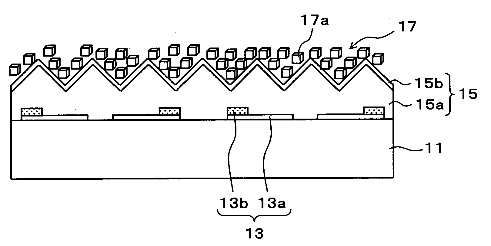
[0018]In the following embodiment, the invention will be explained by exemplifying the case where display electrodes, a dielectric layer, and a layer of magnesium oxide crystals are provided in a front-side substrate assembly, however the case where display electrodes, a dielectric layer, and a layer of magnesium oxide crystals are provided in a rear-side substrate assembly is also included in the scope of the invention.

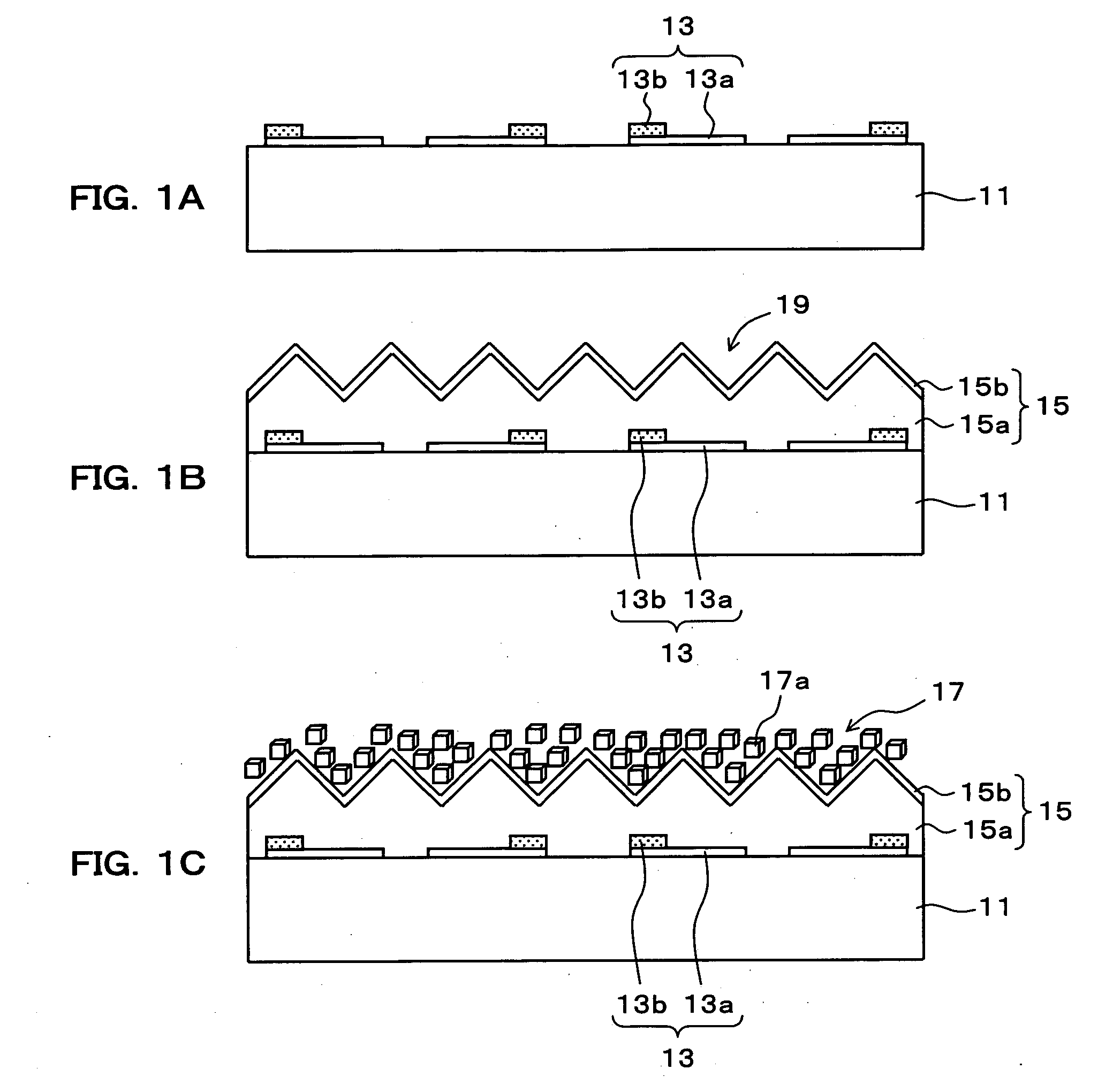
[0019]The method for producing the front-side substrate assembly for a PDP of an embodiment will be described with reference to FIGS. 1A to 1C. FIGS. 1A to 1C are cross-sectional views showing a method for producing the front-side substrate assembly for a PDP of the embodiment. T...


PUM

PropertyMeasurementUnit
particle diameteraaaaaaaaaa
roughness Rzaaaaaaaaaa

Abstract

A method for producing a substrate assembly for a plasma display panel includes the steps of applying a suspension to a dielectric layer covering display electrodes formed on a substrate, the suspension containing a dispersion medium and a large number of magnesium oxide crystals dispersed in the dispersion medium, and thereafter evaporating the dispersion medium to form a layer of the magnesium oxide crystals on the dielectric layer, wherein the dielectric layer has a rugged surface structure having uniformly-dispersed projections and depressions, the rugged surface structure being capable of trapping the magnesium oxide crystals.

Description

CROSS-REFERENCE TO RELATED APPLICATION[0001]This application is related to Japanese Patent Application No. 2006-227001 filed on Aug. 23, 2006, whose priory is claimed and the disclosure of which is incorporated by reference in its entirety.BACKGROUND OF THE INVENTION[0002]1. Field of the Invention[0003]The invention relates to a method for producing a substrate assembly for a plasma display panel (hereinafter, referred to as PDP) and a PDP.[0004]2. Description of the Related Art[0005]FIG. 2 is a perspective view showing a structure of a conventional PDP. The PDP has a structure formed by sticking a front-side substrate assembly 1 and a rear-side substrate assembly 2 to each other. The front-side substrate assembly 1 comprises a front-side substrate 1a, which is a glass substrate, display electrodes 3 each composed of a transparent electrode 31 and a bus electrode 32 and arranged on the substrate 1a, and a dielectric layer 4 covering the display electrodes 3. Further, a protective la...

Claims


Application Information

Patent Timeline
Patent Type & Authority Applications(United States)
IPC IPC(8): B05D3/00H02B1/015H01J9/02H01J11/12H01J11/22H01J11/24H01J11/26H01J11/34H01J11/36H01J11/38H01J11/40H01J11/42H01J11/50
CPCG09G3/298G09G2300/0426H01J11/40H01J11/12H01J11/38H01J9/02H01J9/24
Inventor KASAHARA, SHIGEO
Owner FUJITSU HITACHI PLASMA DISPLAY LTD
Why Eureka
Try Eureka