Scheduling method for processing equipment

a processing equipment and scheduling method technology, applied in the field of integrated processing, can solve the problems of limiting the throughput of the processing sequence, cluster tool users and manufacturers spend a large amount of time, and the time is too long, so as to increase the processing throughput of multiple lots of semiconductor wafers, minimize time gaps, and maintain constant wafer history

Inactive Publication Date: 2008-02-28
APPLIED MATERIALS INC
View PDF41 Cites 30 Cited by
  • Summary
  • Abstract
  • Description
  • Claims
  • Application Information

AI Technical Summary

Benefits of technology

[0012] In one embodiment a method for increasing the processing throughput of multiple lots of semiconductor wafers through a cluster tool while maintaining a constant wafer history for each lot is provided. A first lot of wafers containing one through n-th wafers is introduced into a cluster tool containing one or more processing chambers. The first lot of wafers is processed for a first time period. A second lot of wafers containing one through n-th wafers is introduced into the cluster tool prior to completion of the first time period, wherein the second lot is introduced so as to minimize a time gap between the n-th wafer of the first lot of wafers and the first wafer of the second lot of wafers while maintaining a first constant wafer history for each wafer within the first lot and maintaining a second constant wafer history for each wafer in the second lot. The second lot of wafers is processed for a second time period during at least a portion of the first time period.

Problems solved by technology

In an effort to reduce CoO, electronic device manufacturers often spend a large amount of time trying to enhance the process sequence and chamber processing time to achieve the greatest substrate throughput possible given the cluster tool architecture limitations and the chamber processing times. In track lithography type cluster tools, since the chamber processing times tend to be rather short, (e.g., about a minute to complete the process) and the number of processing steps required to complete a typical process sequence is large, a significant portion of the time it takes to complete the processing sequence is taken up transferring the substrates between the various processing chambers.
If the substrate throughput in a cluster tool is not robot limited, the longest process recipe step will generally limit the throughput of the processing sequence.
This is usually not the case in track lithography process sequences, due to the short processing times and large number of processing steps.
These factors are very important to a cluster tool's profitability and / or usefulness, since the longer the system is unable to process substrates the more money is lost by the user due to the lost opportunity to process substrates in the cluster tool.
Therefore, cluster tool users and manufacturers spend a large amount of time trying to develop reliable processes, reliable hardware, and reliable systems that have increased uptime.
The push in the industry to shrink the size of semiconductor devices to improve device processing speed and reduce the generation of heat by the device, has caused the industry's tolerance to process variability to diminish.
Due to the shrinking size of semiconductor devices and the ever increasing device performance requirements, the allowable variability of the device fabrication process uniformity and repeatability has greatly decreased.
Lithography type device fabrication processes can be especially sensitive to variations in process recipe variables and the timing between the recipe steps, which directly affects process variability and ultimately device performance.

Method used


Image

  • Scheduling method for processing equipment
  • Scheduling method for processing equipment
  • Scheduling method for processing equipment

Examples


example

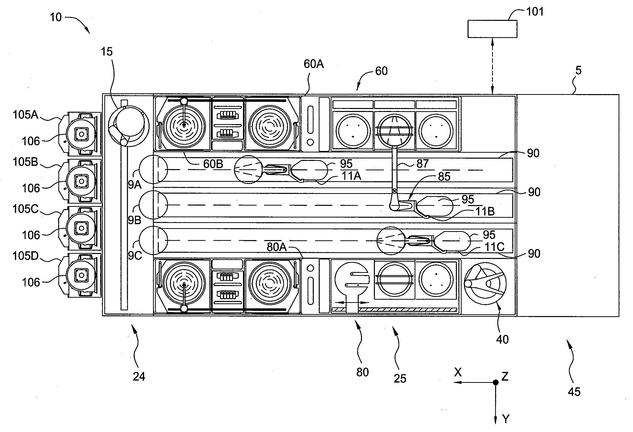
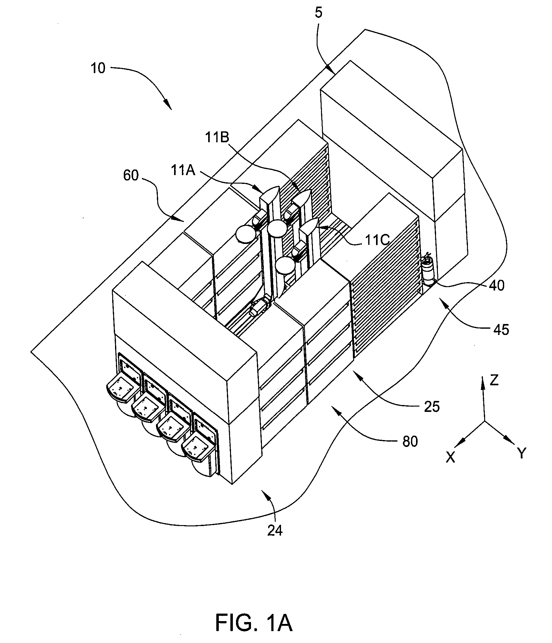
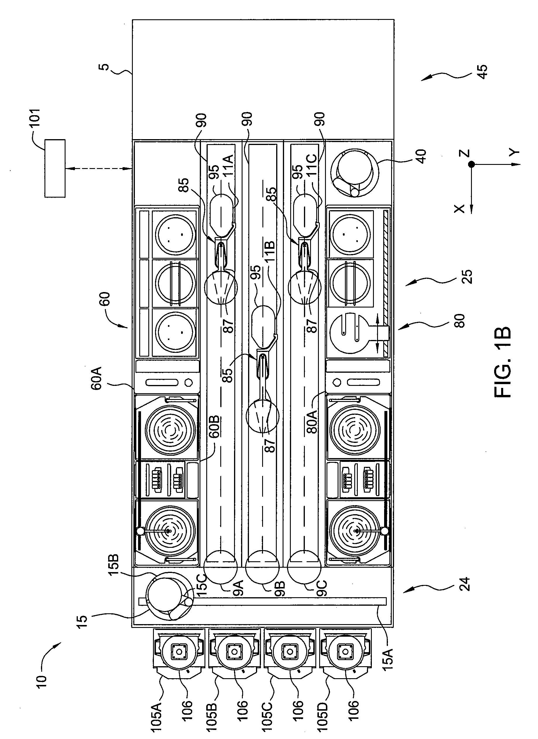
[0112] Examples of the above introduced offline application are further described with reference to FIGS. 6-9. FIG. 6 illustrates an exemplary process flow diagram 1600 describing an example of the rules referred to in step 1520, used to, through software stored in the memory of a controller and some user input, create a schedule for a track system. Although the current example refers to cluster tool 10 with a three robot configuration, it should be noted that the three robot configuration is used only for illustrative purposes, and the offline application and rules can be used to develop schedules for other chambers, for example, chambers containing one, two, or four robot configurations.

[0113] In step 1605, the process begins by examining and inputting the process chamber layout, robot access zones and other system constraints into the offline application software. The input data may be in the form of 3-dimensional positional data of process chamber information (e.g., entrance in...


PUM


Abstract

Methods and apparatus for increasing the processing throughput of multiple lots of semiconductor wafers through a cluster tool while maintaining a constant wafer history for each lot are provided. A first lot of wafers containing one through n-th wafers is introduced into a cluster tool containing one or more processing chambers. The first lot of wafers is processed for a first time period. A second lot of wafers containing one through n-th wafers is introduced into the cluster tool prior to completion of the first time period, wherein the second lot is introduced so as to minimize a time gap between the n-th wafer of the first lot of wafers and the first wafer of the second lot of wafers while maintaining a first constant wafer history for each wafer within the first lot and maintaining a second constant wafer history for each wafer in the second lot.

Description

CROSS-REFERENCE TO RELATED APPLICATIONS [0001] This application claims benefit of U.S. Provisional Patent Application No. 60 / 806,906, filed Jul. 10, 2006, which is herein incorporated by reference.BACKGROUND OF THE INVENTION [0002] 1. Field of the Invention [0003] Embodiments of the invention as recited in the claims generally relate to an integrated processing system containing multiple processing stations and robots that are capable of processing multiple substrates in parallel. In particular, the invention relates to scheduling methods for an integrated processing system. [0004] 2. Description of the Related Art [0005] The process of forming electronic devices is commonly done in a multi-chamber processing system (e.g., a cluster tool) that has the capability to sequentially process substrates, (e.g., semiconductor wafers) in a controlled processing environment. A typical cluster tool used to deposit (i.e., coat) and develop a photoresist material, commonly known as a track litho...

Claims


Application Information

Patent Timeline
Patent Type & Authority Applications(United States)
IPC IPC(8): G06F17/00
CPCH01L21/67276
Inventor HONGKHAM, STEVE S.ENGLHARDT, ERIC A.RICE, MICHAEL R.ARMER, HELEN R.WANG, CHONGYANG CHRIS
Owner APPLIED MATERIALS INC
Why Eureka
Try Eureka