Variable shaped electron beam lithography system and method for manufacturing substrate

a technology of electron beam lithography and electron beam, which is applied in the direction of material analysis using wave/particle radiation, instruments, nuclear engineering, etc., can solve the problems of increasing the complexity of the lsi pattern shape drawn on the photo-mask, raster scan system has higher drawing accuracy, and the number of lsi pattern shapes tends to be exponentially increased, so as to shorten the total drawing time

Inactive Publication Date: 2008-03-06
LONGITUDE SEMICON S A R L
View PDF9 Cites 52 Cited by
  • Summary
  • Abstract
  • Description
  • Claims
  • Application Information

AI Technical Summary

Benefits of technology

[0016]An object of the present invention is to achieve a drawing figure pattern based on the very small number of divided figures compared to that of a related art in order to largely shorten the total drawing time, in drawing, by the VSB system, a figure pattern including an oblique line figure portion including two opposite, oblique lines, each forming an arbitrary, different angle relative to a coordinate axis in an XY drawing rectangular coordinate system. In addition, “XY drawing rectangular coordinate system” means a rectangular coordinate system for representing the shape and position of a figure pattern to be drawn on a drawn target substrate such as a dry plate or a semiconductor wafer, and a lithography system also has a rectangular coordinate system corresponding to it, and in drawing figure patterns, the rectangular coordinate system is used to control hardware, such as an aperture, based on figure pattern information. Further, “oblique line, each forming an arbitrary, different angle relative to a coordinate axis of the XY drawing rectangular coordinate system” or “oblique side” means that a side of a drawing figure pattern forms an arbitrary angle relative to the X-axis direction / the Y-axis direction in the XY drawing rectangular coordinate system except when it is parallel or vertical.

Problems solved by technology

The raster scan system has higher drawing accuracy, but lower throughput because of a large number of shots.
Nowadays, as an LSI pattern is made finer in higher integration, complexity in an LSI pattern shape drawn on a photo-mask is increased, and also the number of LSI patterns tends to be increased exponentially, as the process generation goes forward.
Of course, if an aperture for drawing obliquely is provided, for now, it may be addressed, but an oblique side with any arbitrary angle may not be covered, then it cannot be an actual solution.
While there have been significant advances in the wiring design of LSI patterns, an element arrangement in a direction that has an arbitrary angle is expected to be a useful means to allow a design region to be used effectively, but this arrangement is not permitted in the current Manhattan System.
However, in addition to drawing a photo-mask having LSI design involving such oblique arrangement, in the case of forming a pattern of MEMS (micro Electro Mechanical Systems) or a pattern of a nanoimprinting mold for an optical element, a complex pattern using many oblique sides with an arbitrary angle has to be drawn.
As the result, in a drawing process using the current VSB lithography system, the number of the divided drawing figures becomes enormous.
Therefore, to improve productivity in this process, the largest, technical challenge is to reduce the number of the divided figures in order to shorten the drawing time.
Therefore, there arises a problem of lack of versatility, because it is difficult to connect with rectangular shaped electron beam shot having four sides along the X / Y-axis direction in the XY drawing rectangular coordinate system.
To shorten the total drawing time, setting a size of a divided rectangular figure to be coarse may be also effective, but on the other hand, approximate accuracy in oblique side portions is degraded, so that it cannot be a fundamental solution.

Method used


Image

  • Variable shaped electron beam lithography system and method for manufacturing substrate
  • Variable shaped electron beam lithography system and method for manufacturing substrate
  • Variable shaped electron beam lithography system and method for manufacturing substrate

Examples


Embodiment Construction

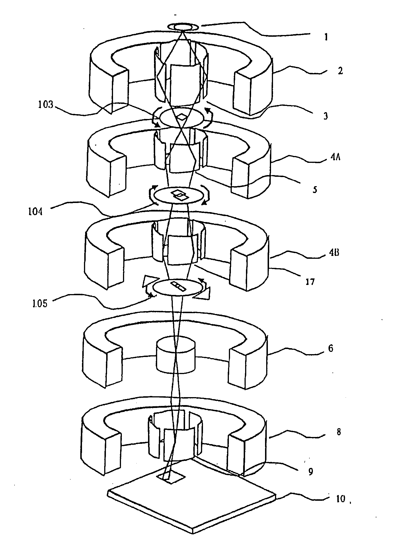
[0048]Now, a description will be provided, using the same symbols with respect to the same functional components in the lithography system (FIG. 2, FIG. 3) described in the related art.

[0049]A lithography system of this exemplary embodiment uses a VSB system. Referring to FIG. 7, an electron gun 1, an illuminating lens system 2, a first aperture 103, a first forming lens system 4A, a second aperture 104, a second forming lens system 4B, a third aperture 105, a reduction lens system 6, an object lens system 8, and a drawn target substrate (a dry plate or a semiconductor wafer) 10 are provided in this order in the beam emission direction of the electron gun 1. In addition, illuminating lens system 2, first forming lens system 4A, second forming lens system 4B, reduction lens system 6, and object lens system 8 respectively have deflectors 3, 5, 17, and 9 for deflecting a beam.

[0050]Each of first aperture 103, second aperture 104 and third aperture 105 for forming an electron beam has a...


PUM

PropertyMeasurementUnit
angleaaaaaaaaaa
arbitrary angleaaaaaaaaaa
angleaaaaaaaaaa

Abstract

This VSB lithography system includes a first, second and third aperture for forming a single electron beam in each of the rectangular opening portion that are provided, and draws a figure pattern using the single electron beam formed by passing the beam through the first, second and third aperture in sequence. Each of the first, second and third aperture has a mechanism for rotationally driving the aperture around an optical axis up to an arbitrary angle from 0 to 360°. Further, in the third aperture, a mechanism for varying the opening slit width of the rectangular opening portion is provided.

Description

[0001]This application is based upon and claims the benefit of priority from Japanese patent application No. 2006-241331, filed on Sep. 6, 2006, the disclosure of which is incorporated herein in its entirety by reference.BACKGROUND OF THE INVENTION[0002]1. Field of the Invention[0003]The present invention relates to a variable shaped electron beam lithography system for drawing a figure pattern including an oblique line with an arbitrary angle by forming a single electron beam shot in the same shape as the figure pattern, and a method for manufacturing a substrate.[0004]2. Description of the Related Art[0005]In a photo mask electron beam lithography system including an electron optical system having a 50 kV electron gun, a raster scan system and a variable shaped beam system (hereinafter, called “VSB system”) have been developed, and at the present day, both of them are put into practical use. The raster scan system is, as shown in FIG. 1A, a system which scans a resist layer of a p...

Claims


Application Information

Patent Timeline
Patent Type & Authority Applications(United States)
IPC IPC(8): H01J37/30
CPCB82Y10/00B82Y40/00H01J37/09H01J37/1472H01J2237/0835H01J37/3174H01J2237/0455H01J2237/0456H01J2237/0458H01J37/3023
Inventor HIROSHIMA, MASAHITO
Owner LONGITUDE SEMICON S A R L
Why Eureka
Try Eureka