Semiconductor device

a technology of mikro-mos transistors and transistors, applied in pulse generators, instruments, pulse techniques, etc., can solve the problems of inability to grasp the variation in the threshold voltage of the transistor by one replica mos transistor, broken dram operation, and inability to control threshold voltage precision, etc., to reduce power consumption and suppress the effect of sense speed

Inactive Publication Date: 2008-03-06
HITACHI LTD
View PDF11 Cites 17 Cited by
  • Summary
  • Abstract
  • Description
  • Claims
  • Application Information

AI Technical Summary

Benefits of technology

[0017]The advantages obtained by the representative features of the present invention described in the present application reside in that it is possible to suppress a decrease in the sense speed or realize the lower power consumption.

Problems solved by technology

As a result, a period of time required when the sense amplifier amplifies the data, and the operation of the DRAM is broken.
However, in that system, because the number of replica MOS transistors is one, there arises such a problem that a precision of the threshold voltage control is lacked.
More specifically, because a large number of sense amplifier MOS transistors of the DRAM are disposed on the chip, it is impossible to grasp a variation in the threshold voltages of the transistor by one replica MOS transistor.
The erroneous threshold voltage control induces such problems that the sense speed is decreased and the power consumption is increased.

Method used


Image

  • Semiconductor device
  • Semiconductor device
  • Semiconductor device

Examples


first embodiment

[0050]Hereinafter, a semiconductor device according to one embodiment of the present invention will be described with reference to FIGS. 1 to 5.

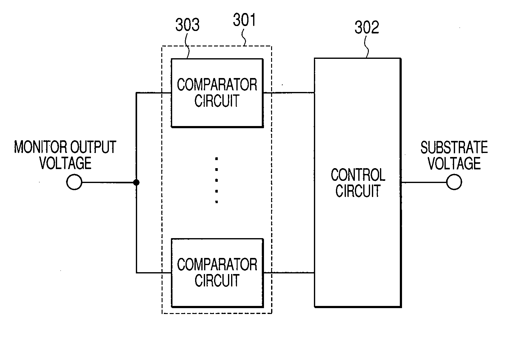
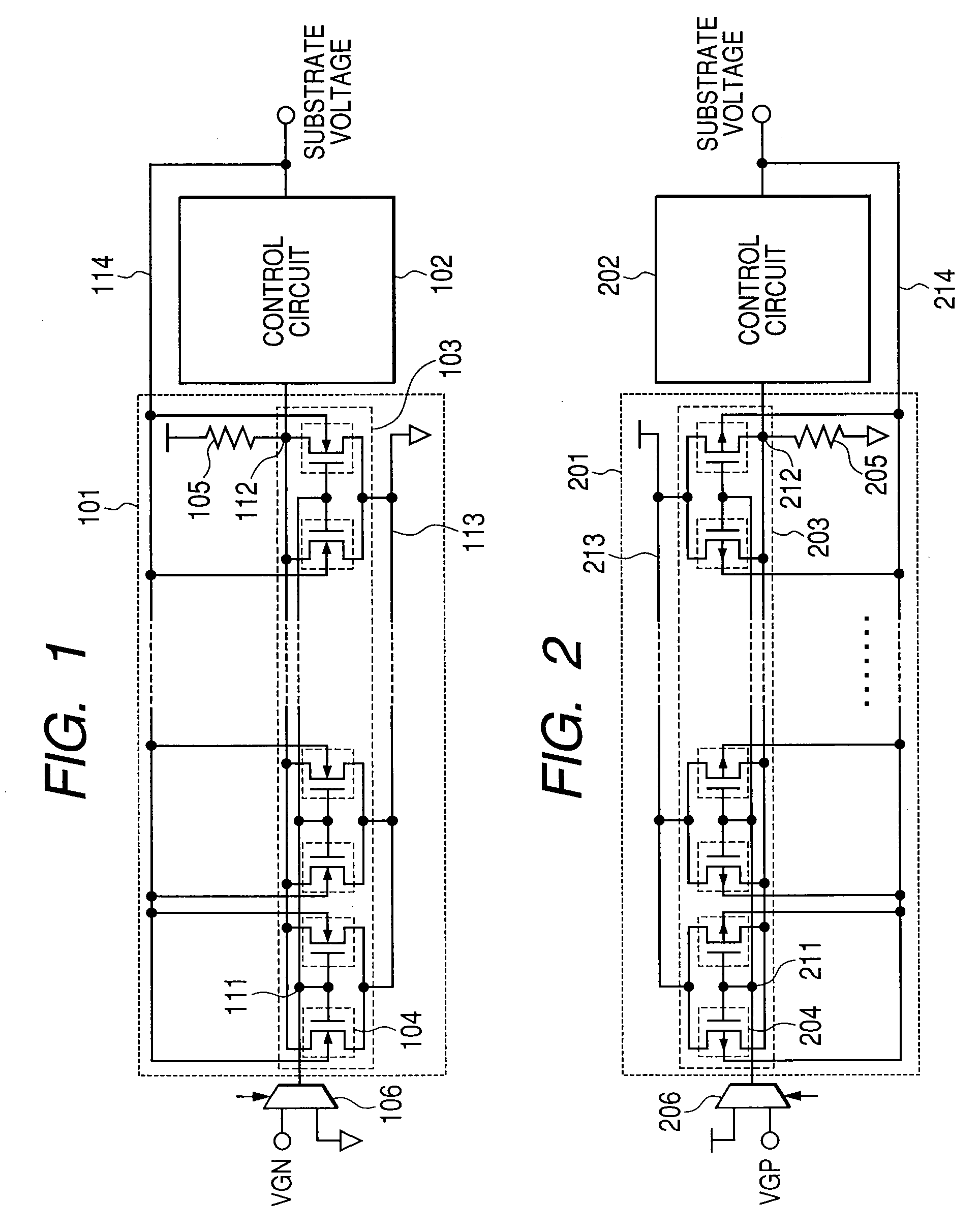
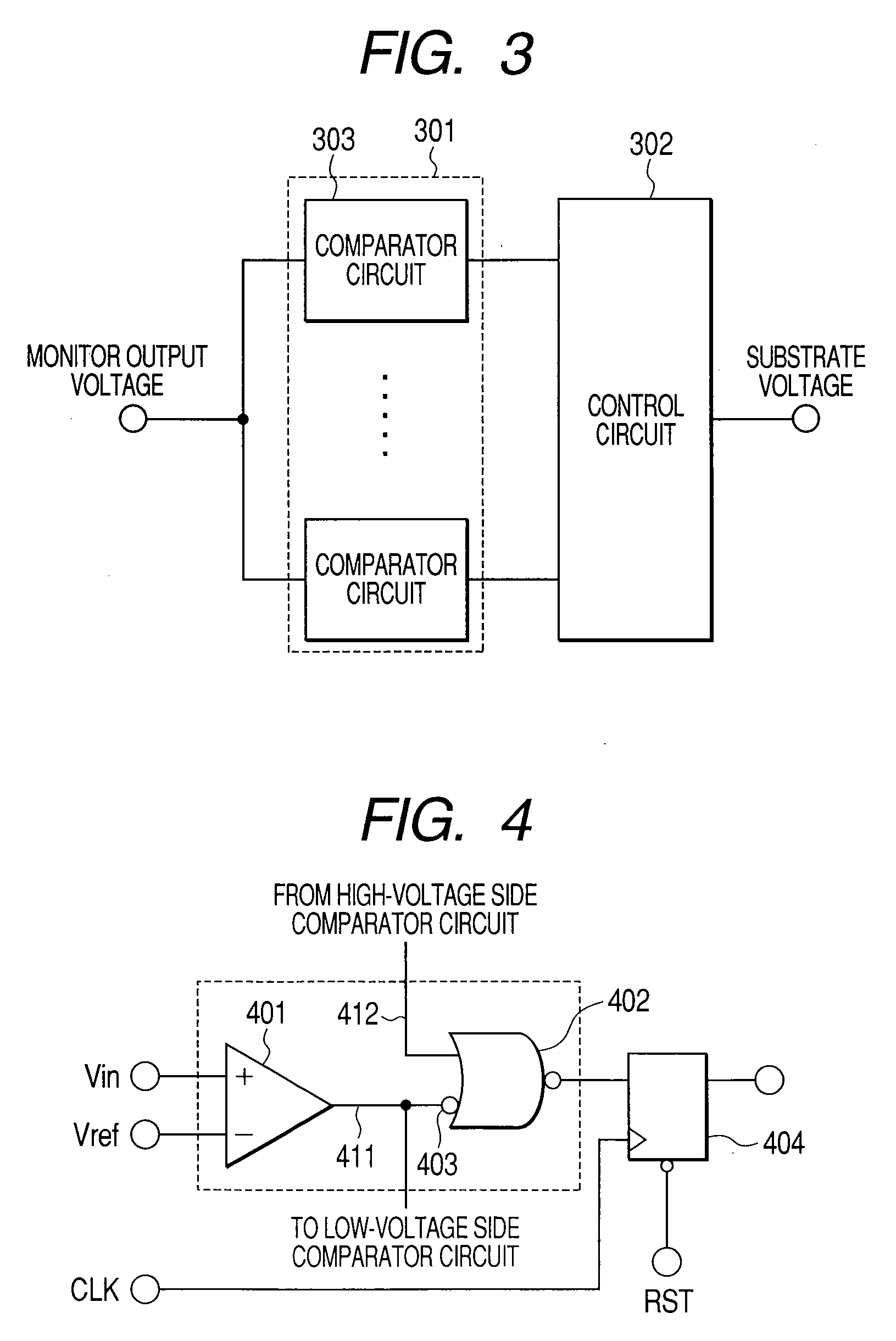
[0051]FIG. 1 is a block diagram showing an entire NMOS transistor substrate control circuit. The NMOS transistor substrate control circuit is roughly classified into two circuits. One circuit is a sense amplifier NMOS transistor threshold voltage monitoring circuit 101, and another circuit is a control circuit 102.

[0052]The NMOS transistor threshold voltage monitoring circuit 101 includes a replica NMOS transistor array 103 and a resistor 105. The replica NMOS transistor array 103 is composed of plural replica NMOS transistors 104. All gate terminals of those plural replica NMOS transistors 104 are connected to a node 111, all drain terminals thereof are connected to a node 112, all source terminals thereof are connected to a node 113, and all substrates are connected to a node 114. The node 111 is input with a gate input voltage VGN. The ga...

second embodiment

[0089]FIG. 14 is a diagram showing the entire block of a semiconductor device according to another embodiment of the present invention. A difference from the first embodiment resides in that variation control circuits 153 and 154 are added. The variation control circuits detect variations in the threshold voltages of the sense amplifier NMOS / PMOS transistors within the chip according to the outputs from the entire NMOS (PMOS) substrate control blocks (sense amplifier NMOS / PMOS transistor threshold voltage monitoring circuits 151 and the control circuits 152) shown in FIGS. 1 and 2, which are disposed in plurality within the DRAM chip, and control the substrate voltage of the entire chip to control the threshold voltages. As a result, it is possible to adjust the sense speed at an optimum speed, and it is possible to reduce the power consumption. The sense amplifier NMOS / PMOS transistor threshold voltage monitoring circuit 151 shown in FIG. 14 which will be described later is substan...


PUM


Abstract

A substrate voltage control technique that prevents the operating speed from being decreased and suppresses a leakage current due to a lower threshold voltage with respect to a low voltage use. Since a center value of the threshold voltages is detected by plural replica MOS transistors, and a substrate voltage is controlled to control a center value of the threshold voltages, thereby making it possible to satisfy a lower limit of the operating speed and an upper limit of a leakage current of the entire chip. On the other hand, the substrate voltage is dynamically controlled during the operation of the chip, thereby making it possible to decrease the center value of the threshold voltages when the chip operates to improve the speed, and to increase the center value of the threshold voltages after the operation of the chip to reduce the leakage current of the entire chip.

Description

CLAIM OF PRIORITY[0001]The present application claims priority from Japanese application JP 2006-234896 filed on Aug. 31, 2006, the content of which is hereby incorporated by reference into this application.FIELD OF THE INVENTION[0002]The present invention relates to a semiconductor device, and more particularly to a semiconductor memory device that is effective in reducing a variation in a threshold voltage of a sense amplifier of the semiconductor memory device, and a control method therefor.BACKGROUND OF THE INVENTION[0003]According to the studies of the present inventors, there have been proposed the following control technique for the semiconductor device.[0004]For example, dynamic random access memories (hereinafter referred to as “DRAM”) that is one of the semiconductor devices have been incorporated in large numbers into diverse electronic devices that are used by us usual day. Also, with the low power consumption of the devices and the needs for the high performance in rece...

Claims


Application Information

Patent Timeline
Patent Type & Authority Applications(United States)
IPC IPC(8): H01L23/58
CPCG11C5/146G11C11/401G11C11/4074G11C29/02G11C29/026H01L2924/0002G11C29/028H01L2924/00
Inventor NAKAYA, HIROAKIAKIYAMA, SATORUSEKIGUCHI, TOMONORITAKEMURA, RIICHIRO
Owner HITACHI LTD
Why Eureka
Try Eureka