Carrier board structure with semiconductor chip embedded therein

a carrier board and semiconductor chip technology, applied in the direction of printed circuit manufacturing, printed circuit aspects, basic electric elements, etc., can solve the problems of limiting the use of such a package structure, difficult to dispose of semiconductor chips in the cavity, and difficult to sufficiently and evenly fill the narrow slit between the semiconductor chip and the cavity by the adhesion material, so as to facilitate the disposing of semiconductor chips

Inactive Publication Date: 2008-03-06
PHOENIX PRECISION TECH CORP
View PDF3 Cites 27 Cited by
  • Summary
  • Abstract
  • Description
  • Claims
  • Application Information

AI Technical Summary

Benefits of technology

[0018]Compared with the prior art, the cavity of the carrier board structure of the present invention has a chamfer, which not only facilitates disposing the semiconductor chip in the cavity, but also allows the adhesion material to be evenly

Problems solved by technology

Although such a package structure enables a higher pin count per unit area, in high frequency or high speed application, its long electrical conducting path leads to high resistance and prevents further improvement of electrical characteristic, thereby limiting the use of such a package structure.
However, the vertical cavity of the same size from top to bottom in the above structures makes it difficult to dispose the semiconductor chip in the cavity.
In addition, it is difficult to sufficiently and evenly fill the narrow slit between the semiconductor chip and the cavity by the adhesion material.
As a result, the air and voids can be left in the cavity, and the residual vo

Method used


Image

  • Carrier board structure with semiconductor chip embedded therein
  • Carrier board structure with semiconductor chip embedded therein
  • Carrier board structure with semiconductor chip embedded therein

Examples


Embodiment Construction

[0023]The present invention relates generally to a carrier board structure, and more particularly to a carrier board structure with a semiconductor chip embedded therein. The following description is presented to enable one of ordinary skill in the art to make and use the invention and is provided in the context of a patent application and its requirements. Various modifications to the preferred embodiments and the generic principles and features described herein will be readily apparent to those skilled in the art. Thus, the present invention is not intended to be limited to the embodiments shown, but is to be accorded the widest scope consistent with the principles and features described herein.

[0024]FIGS. 3A to 3E show a fabrication process of a carrier board structure with a semiconductor chip embedded therein according to a first embodiment of the present invention.

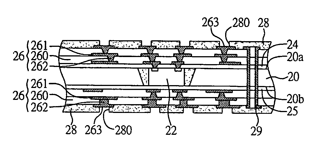
[0025]As shown in FIG. 3A, a carrier board 20 with a first surface 20a and a second surface 20b opposed to the fir...


PUM


Abstract

A carrier board structure with semiconductor chip embedded therein is proposed. The carrier board structure includes a carrier board having a first surface and a second surface opposed to the first surface, wherein the carrier board including at least one cavity having a chamfer. A semiconductor chip can be easily disposed in the cavity by the chamfer, and an adhesion material can be evenly filled in the cavity by the chamfer, so as to avoid generating air bubbles, voids and reduce stress.

Description

CROSS-REFERENCE TO RELATED APPLICATIONS[0001]The present application is related to co-pending Taiwan Application No. 095118215, filed on May 23, 2006.FIELD OF THE INVENTION[0002]The present invention relates generally to a carrier board structure, and more particularly to a carrier board structure with a semiconductor chip embedded therein.DESCRIPTION OF RELATED ART[0003]With rapid development of semiconductor package technology, there have been developed various kinds of package structures for semiconductor devices. To form a semiconductor device package structure, a semiconductor chip is typically mounted to and electrically connected with a package substrate or a lead frame and then encapsulated by an encapsulant. In BGA semiconductor packaging, a semiconductor chip is mounted to and electrically connected to a package substrate. The back side of the package substrate has an array solder balls formed through a self-alignment technology, by which electrical connection can be made ...

Claims


Application Information

Patent Timeline
IPC IPC(8): H01L23/04
CPCH01L23/49827H01L24/19H01L24/24H01L24/82H01L2224/24227H01L2924/01027H01L2924/01078H01L2924/01082H01L2924/15153H01L2924/15165H01L2924/18162H05K1/185H05K3/4602H05K2201/0187H05K2201/09827H05K2201/10674H01L23/5389H01L2924/014H01L2924/01033H01L2924/351H01L2924/00
Inventor SHIH, CHAO-WEN
Owner PHOENIX PRECISION TECH CORP
Why Eureka
Try Eureka