Semiconductor Device and Fabricating Method Thereof

a technology of semiconductor devices and dielectric barriers, which is applied in the direction of semiconductor devices, semiconductor/solid-state device details, electrical equipment, etc., can solve the problems of reducing the yield of a process, increasing the cost, and affecting so as to improve the reliability and characteristics of the device, enhance the adhesion properties between a metal layer and a dielectric barrier layer.

Inactive Publication Date: 2008-03-06
DONGBU HITEK CO LTD
View PDF5 Cites 0 Cited by
  • Summary
  • Abstract
  • Description
  • Claims
  • Application Information

AI Technical Summary

Benefits of technology

[0006]Embodiments of the present invention provide a semiconductor device and a fabricating method thereof. Adhesive properties between a metal layer and a dielectric barrier layer can be enhanced, thereby improving the reliability and characteristics of the device.

Problems solved by technology

However, the use of a dielectric barrier often causes a peeling phenomenon during a pad process when a semiconductor is fabricated.
This lowers the yield of a process and raises the costs.
Also, an aluminum (Al) pad may not be able to be directly connected a Cu metal interconnection due to the peeling.

Method used


Image

  • Semiconductor Device and Fabricating Method Thereof
  • Semiconductor Device and Fabricating Method Thereof

Examples


Embodiment Construction

[0011]When the terms “on” or “over” are used herein, when referring to layers, regions, patterns, or structures, it is understood that the layer, region, pattern or structure can be directly on another layer or structure, or intervening layers, regions, patterns, or structures may also be present. When the terms “under” or “below” are used herein, when referring to layers, regions, patterns, or structures, it is understood that the layer, region, pattern or structure can be directly under the other layer or structure, or intervening layers, regions, patterns, or structures may also be present.

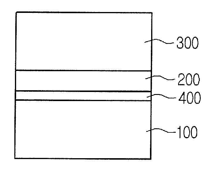
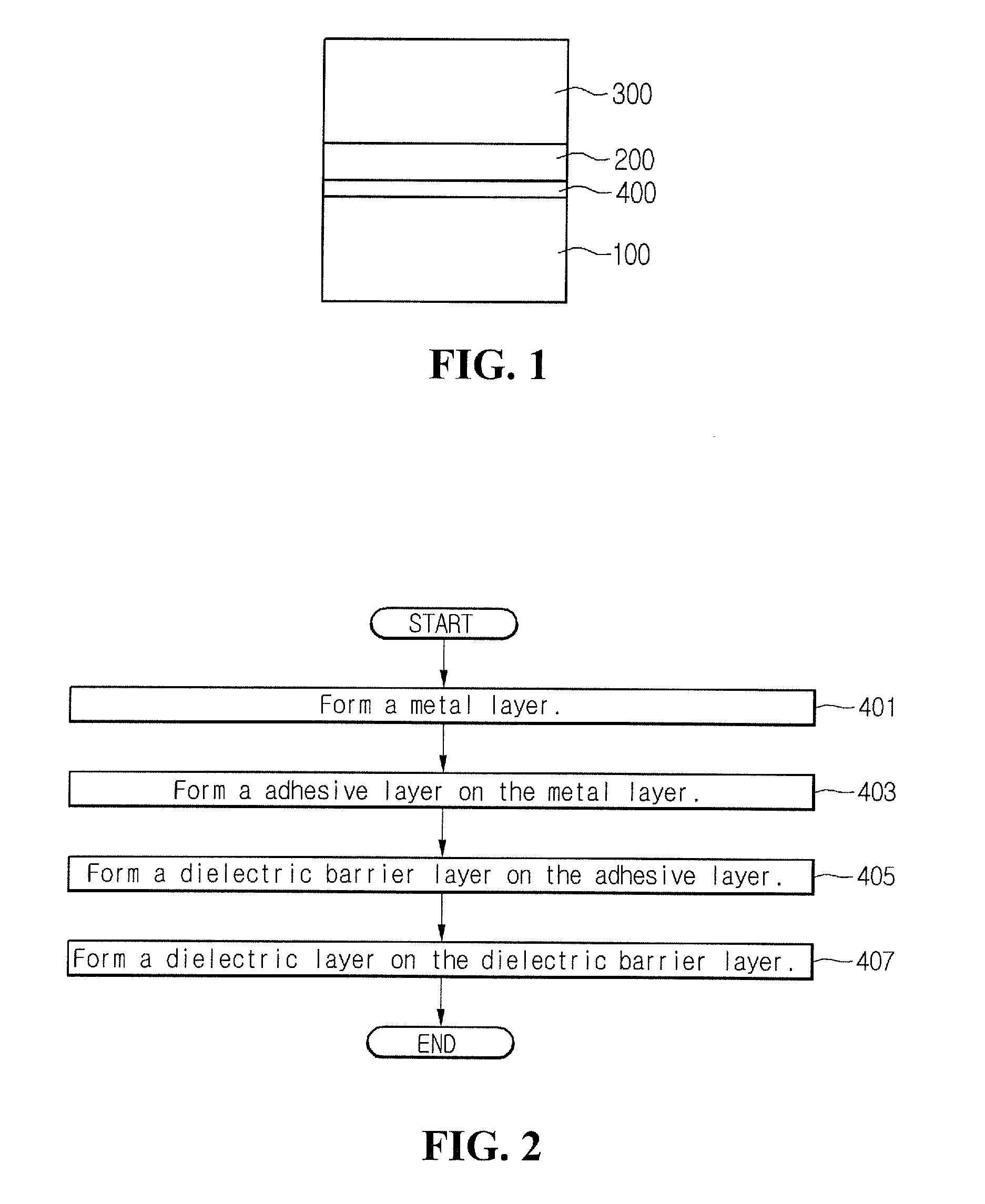
[0012]Referring to FIG. 1, an Inter Layer Dielectric (ILD) layer according to an embodiment of the present invention can include a metal layer 100, an adhesive layer 400, a dielectric barrier layer 200, and a dielectric layer 300.

[0013]The metal layer 100 can be used for forming an interconnection. For example, the metal layer 100 can include copper (Cu) to be able to form an interconnection of...


PUM

PropertyMeasurementUnit
dielectric constantaaaaaaaaaa

Abstract

A semiconductor device and fabricating method thereof are disclosed. An adhesive layer is provided between a metal layer and a dielectric barrier layer. A dielectric layer having a low dielectric constant is formed on the dielectric barrier layer.

Description

CROSS-REFERENCE TO RELATED APPLICATION[0001]The present application claims the benefit under 35 U.S.C. §119 of Korean Patent Application No. 10-2006-0083865, filed Aug. 31, 2006, which is hereby incorporated by reference in its entirety.BACKGROUND[0002]Semiconductor devices typically include a metal interconnection and a dielectric layer. Often, a dielectric barrier is used to inhibit the metal layer from diffusing into the dielectric layer. For example, a metal interconnection of a semiconductor device may include copper (Cu), and SiN may be used for a dielectric barrier that inhibits Cu from diffusing.[0003]In addition, the dielectric barrier, employed to enhance the performance of a highly integrated device, typically has a low dielectric constant.[0004]However, the use of a dielectric barrier often causes a peeling phenomenon during a pad process when a semiconductor is fabricated. This lowers the yield of a process and raises the costs. Also, an aluminum (Al) pad may not be abl...

Claims


Application Information

Patent Timeline
Patent Type & Authority Applications(United States)
IPC IPC(8): H01L23/48H01L21/4763
CPCH01L21/76832H01L23/53295H01L23/5329H01L21/76834H01L2924/0002H01L2924/00H01L21/28
Inventor SHIM, CHEON MAN
Owner DONGBU HITEK CO LTD
Why Eureka
Try Eureka