Electrooptic device, driving circuit, and electronic device

Active Publication Date: 2008-03-06
JAPAN DISPLAY WEST
View PDF1 Cites 26 Cited by
  • Summary
  • Abstract
  • Description
  • Claims
  • Application Information

AI Technical Summary

Benefits of technology

[0006]An advantage of some aspects of the invention is to provide an electrooptic device, a driving circuit thereof, and an electronic device

Problems solved by technology

However, since this technique employs a structure in which a capacitor-line driving circuit and a scanning-line driving circuit (

Method used


Image

  • Electrooptic device, driving circuit, and electronic device
  • Electrooptic device, driving circuit, and electronic device
  • Electrooptic device, driving circuit, and electronic device

Examples


first embodiment

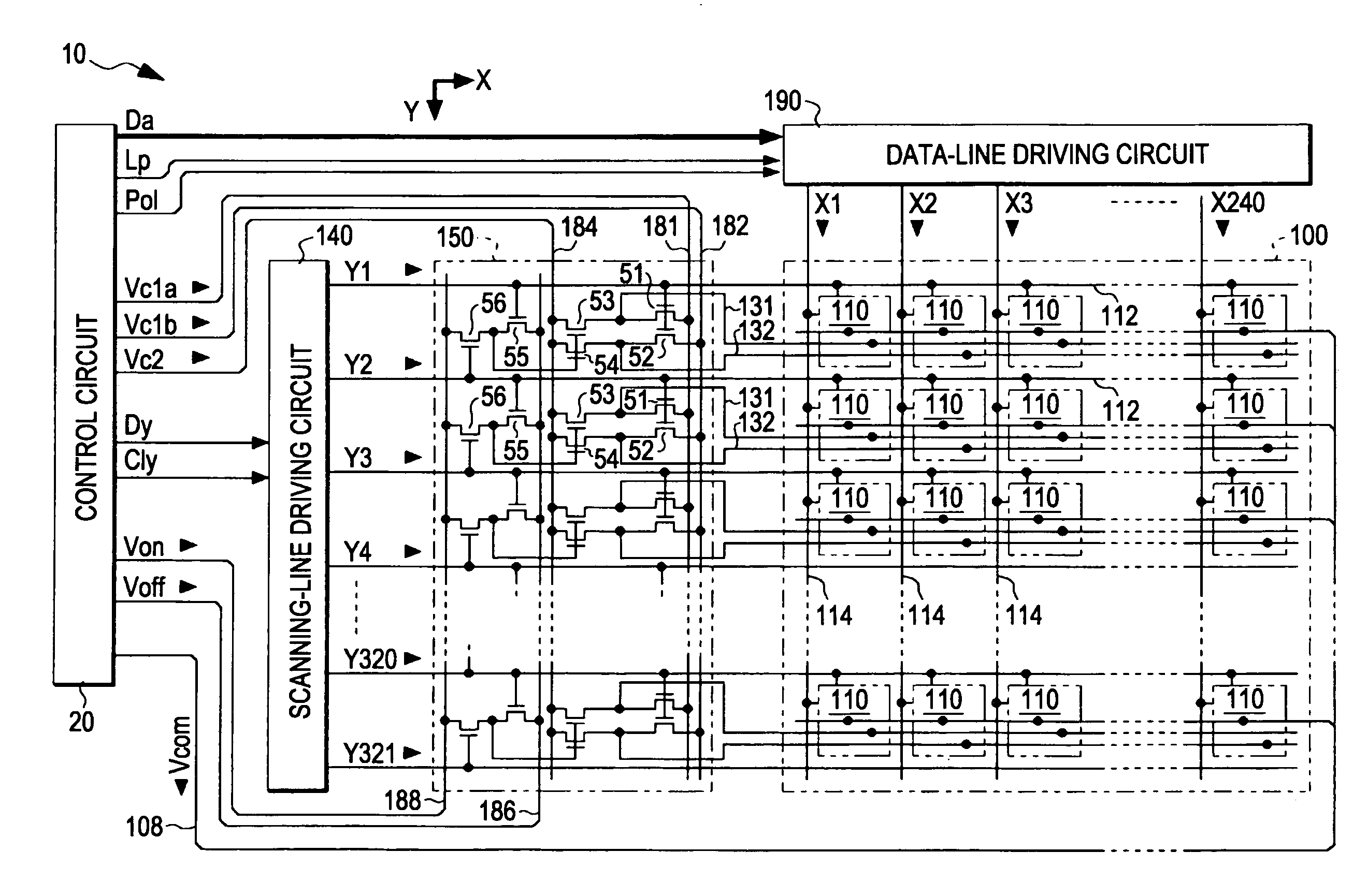
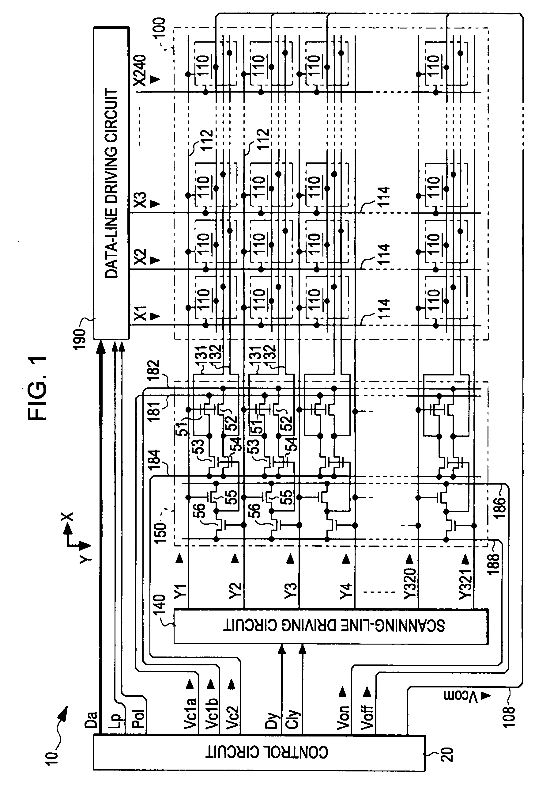
[0038]A first embodiment of the invention will first be described. FIG. 1 is a block diagram of an electrooptic device according to a first embodiment of the invention.

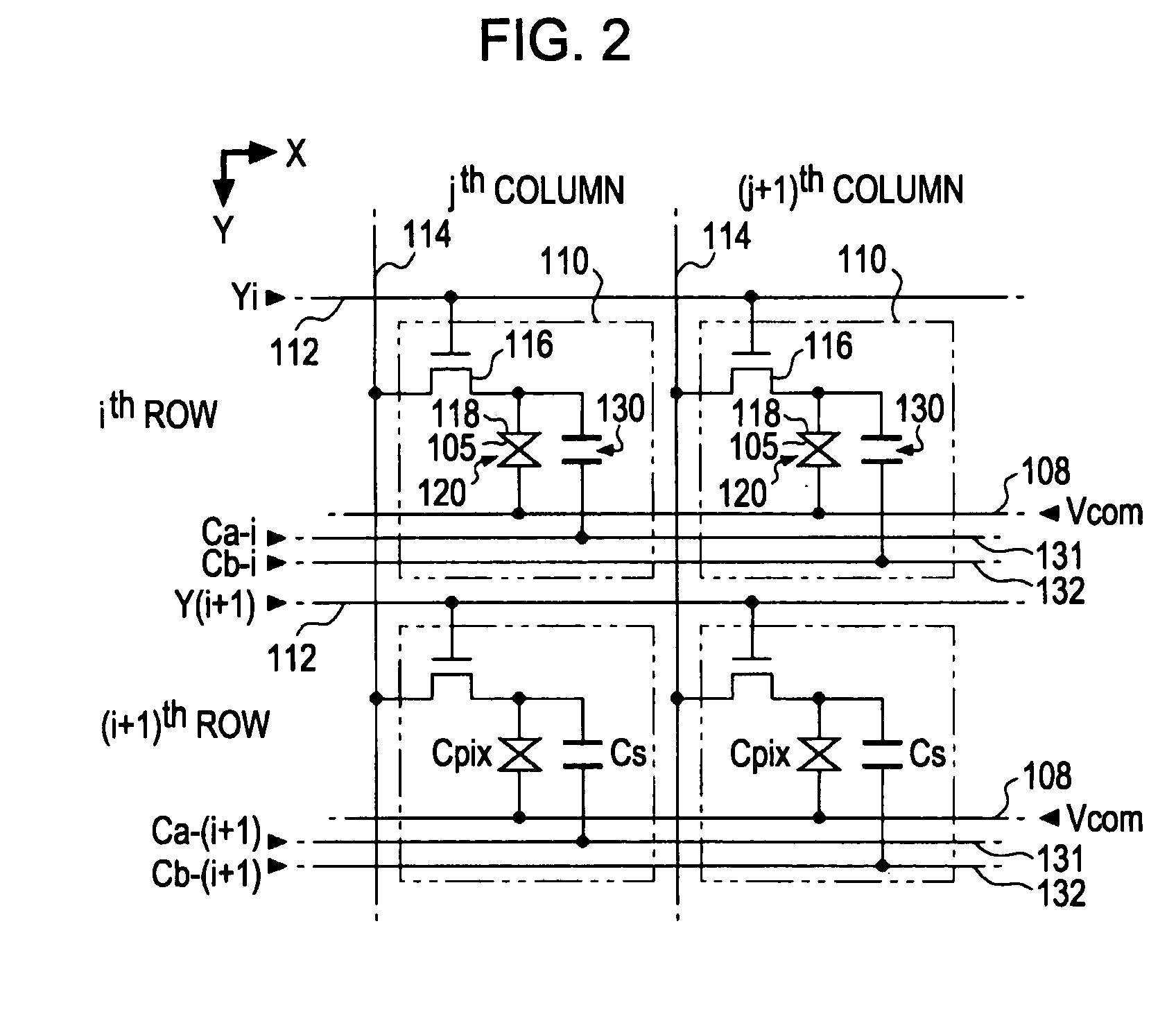
[0039]As shown in the diagram, the electrooptic device, denoted at 10, has a display region 100, and a control circuit 20, a scanning-line driving circuit 140, a capacitor-line driving circuit 150, and a data-line driving circuit 190 around the display region 100. The display region 100 has an array of pixels 110, in which 321 scanning lines 112 extend transversely (in the X direction) and 240 data lines extend longitudinally (in the Y direction). The pixels 110 are disposed at the intersections of the first to 320th scanning lines 112 and the first to 240th data lines 114. Accordingly, in this embodiment, the pixels 110 are arrayed in a 320 by 240 matrix in the display region 100. The invention is not however limited to that matrix.

[0040]In this embodiment, the 321st scanning line 112 does not contribute to the verti...

second embodiment

[0158]A second embodiment of the invention will be described. FIG. 14 is a block diagram of an electrooptic device according to the second embodiment; and FIG. 15 is a plan view of the boundary between the capacitor-line driving circuit 150 and the display region 100 of the device substrate.

[0159]The second embodiment is different from the first embodiment shown in FIG. 1 (FIG. 3) in the following points: the configuration of the capacitor-line driving circuit 150 (a first difference); there is no third feed line (a second difference); the relationship between the line to which the second end of the storage capacitor 130 is connected and the capacitor line (a third difference); and the common signal Vcom applied to the common electrode 108 is not constant in voltage (a fourth difference).

[0160]The second embodiment will be described centering on these differences.

[0161]The first and second differences will first be described. The capacitor-line driving circuit 150 of the second embo...


PUM


Abstract

A driving circuit of an electrooptic device includes: a plurality of scanning lines; a plurality of data lines; first and second capacitor lines; a common electrode; pixels; a scanning-line driving circuit; a capacitor-line driving circuit; and a data-line driving circuit. The pixels each include: a pixel switching element; a pixel capacitor disposed between the pixel switching element and the common electrode; and a storage capacitor. When the one scanning line is selected, the capacitor-line driving circuit shifts the voltage of a first (or second) capacitor line corresponding to one scanning line to one of higher and lower levels from a predetermined voltage by a predetermined value, and holds the predetermined voltage after a scanning line apart from the one scanning line by a predetermined number of lines is selected until the one scanning line is selected again.

Description

BACKGROUND[0001]1. Technical Field[0002]The present invention relates to a technique for electrooptic devices such as liquid crystal devices to reduce the voltage amplitude of the data lines and to achieve high-definition display.[0003]2. Related Art[0004]Electrooptic devices such as liquid crystal devices have pixel capacitors (liquid-crystal capacitors) corresponding to the intersections of scanning lines and data lines. When there is a need to drive the pixel capacitors by an alternating current, the components of a data-line driving circuit which provides data signals to the data lines are required to have resistance to voltage corresponding to the voltage amplitude of the data signals, because the voltage amplitude has positive and negative polarities. To meet this need, there is proposed a technique for reducing the voltage amplitude of the data signals by providing storage capacitors in parallel to the pixel capacitors and by driving capacitor lines connected to a common stor...

Claims


Application Information

Patent Timeline
IPC IPC(8): G06F3/038G09G3/20
CPCG09G3/3614G09G2300/0876G09G3/3677G09G3/3655
Inventor YAMAZAKI, KATSUNORI
Owner JAPAN DISPLAY WEST
Why Eureka
Try Eureka