Liquid crystal display device
a liquid crystal display and display device technology, applied in non-linear optics, instruments, optics, etc., can solve the problems of unintentional gap left in coating, uneven coating, and uneven coating in particular directions, so as to prevent display quality from being deteriorated, prevent coating unevenness of colored layer, and reduce manufacturing yield
- Summary
- Abstract
- Description
- Claims
- Application Information
AI Technical Summary
Benefits of technology
Problems solved by technology
Method used
Image
Examples
first embodiment
[0028]Descriptions will be given below of a first embodiment of the present invention with reference to the accompanying drawings.
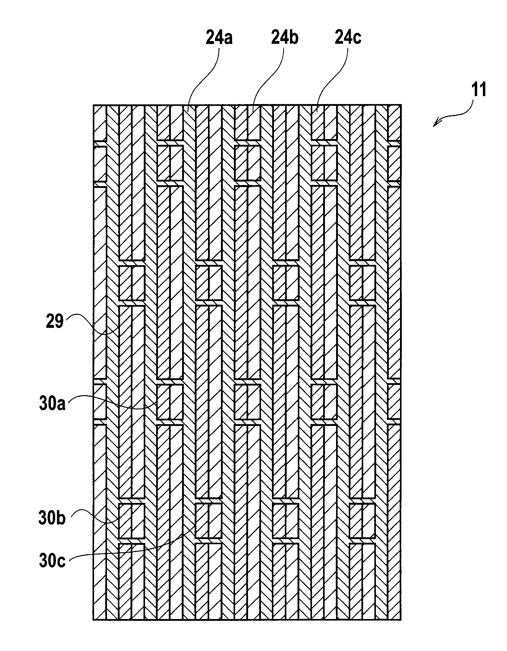
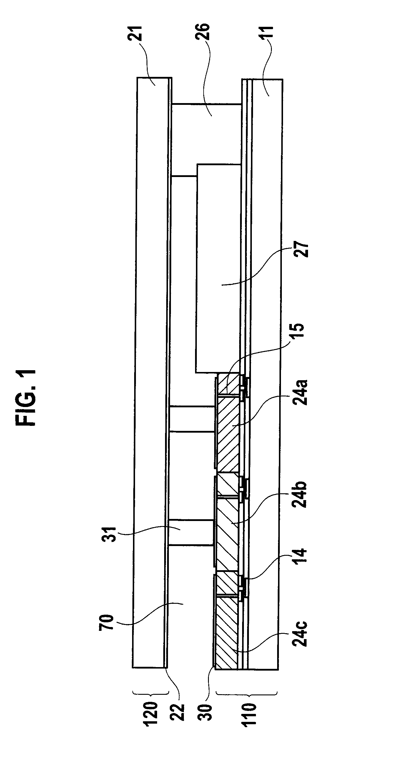
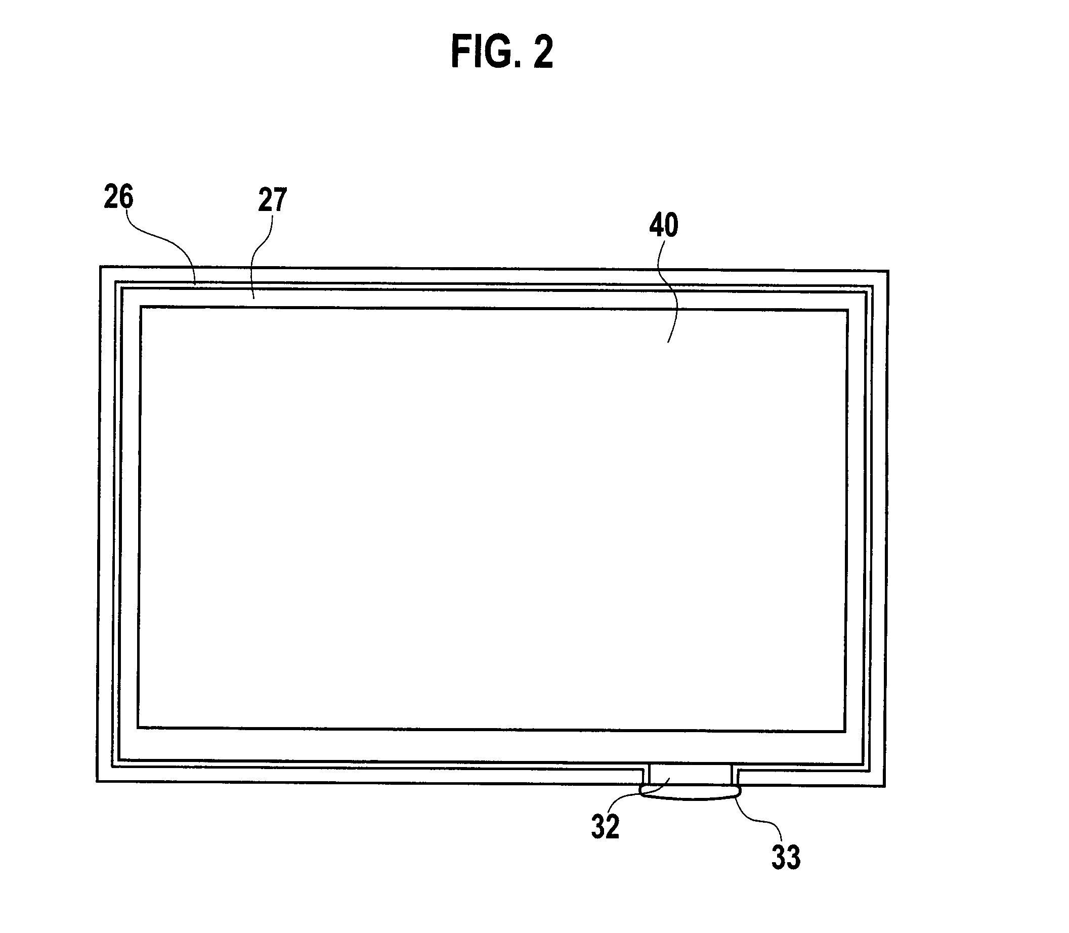
[0029]FIG. 1 is a configurational view of a liquid crystal display device according to an embodiment of the present invention. FIG. 2 is an overview showing a display area and also the entire configuration of the liquid crystal display device according to the embodiment. As shown in FIG. 1, the liquid crystal display device includes an array substrate 110 and an opposite substrate 120. The array substrate 110 includes colored layers 24a, 24b and 24c. A liquid crystal layer 70 is held between the array substrate 110 and the opposite substrate 120. The distance between the array substrate 110 and the opposite substrate 120 is maintained by columnar spacers 31 each formed of resin.
[0030]As shown in FIG. 2, the opposite substrate 120 and the array substrate 110 are bonded to each other with a seal 26, which is disposed in a manner of surrounding the outer per...
second embodiment
[0064]FIG. 11 shows an example of a mask pattern of the first colored layer 24a of this embodiment. The mask pattern shown in FIG. 11 is formed by omitting the grid squares 28 of predetermined pixels from a grid pattern shown in FIG. 4.
[0065]In the mask pattern of this embodiment, as shown in FIG. 11, grid squares are omitted in 6 out of every 8 pixels in the vertical direction (denoted by reference numeral 31). In addition, in the mask pattern shown in FIG. 11, each pixel in which a grid is omitted is displaced with respect to pixels in the adjacent lines each extending in the vertical direction, so that pixels in which grid squares are formed are not successively positioned side by side in the horizontal direction. In other words, a grid 32a is arranged in a manner that the grid 32a is not adjacent to grid squares 32b and 32c in the adjacent lines.
[0066]Specifically, when (n, m) denotes the coordinates of a pixel having a grid square formed therein, grid squares are omitted in pix...
PUM
| Property | Measurement | Unit |
|---|---|---|
| temperature | aaaaa | aaaaa |
| temperature | aaaaa | aaaaa |
| temperature | aaaaa | aaaaa |
Abstract
Description
Claims
Application Information


