Non-volatile semiconductor storage device and non-volatile storage system

Active Publication Date: 2008-03-06
KIOXIA CORP
View PDF6 Cites 54 Cited by
  • Summary
  • Abstract
  • Description
  • Claims
  • Application Information

AI Technical Summary

Benefits of technology

[0010]In One aspect the present invention provides a non-volatile semiconductor memory device comprising: a memory cell array comprising a plurality of memory cells enabled to store multi-value data by differences of threshold voltages, the memory cells being arranged along a plurality of bit-lines and a plurality of word-lines; a sense amplifier circuit connected to the bit-lines; a word-line control circuit controlling applying a read voltage as a word line voltage to the word line, the read voltage being larger than an upper limit of one of plural threshold voltage distributions representing the data and smaller than a lower limit of another threshold voltage distribution with higher threshold voltages than the one of the plural threshold voltage distributions, and applying a soft-value read voltage as a word line voltage to the word line, the soft-value read voltage being smaller than an upper limit of each of the plurality of the threshold voltage distributions and larger than a lower limit thereof to generate a plurality of soft-values; a likelihood calculation circuit calculating a likel

Problems solved by technology

However, a probability of fail bit occurrence in a memory cell array is increasing greatly, as the memory cell is miniaturized, thus lowering the yield of non-volatile memory chips.
Performing a refresh operation in all memory areas results in a long time for finishing a refresh operation.
In addition, it might give an unnecessary stress to areas with a small amount of fail bits.
Moreover, in an error-correction process using iterative decoding method based on soft-decision information, it is difficult to judge whether the number of error corrections conducted is close to a limit correctable by an error correction code.

Method used


Image

  • Non-volatile semiconductor storage device and non-volatile storage system
  • Non-volatile semiconductor storage device and non-volatile storage system
  • Non-volatile semiconductor storage device and non-volatile storage system

Examples


second embodiment

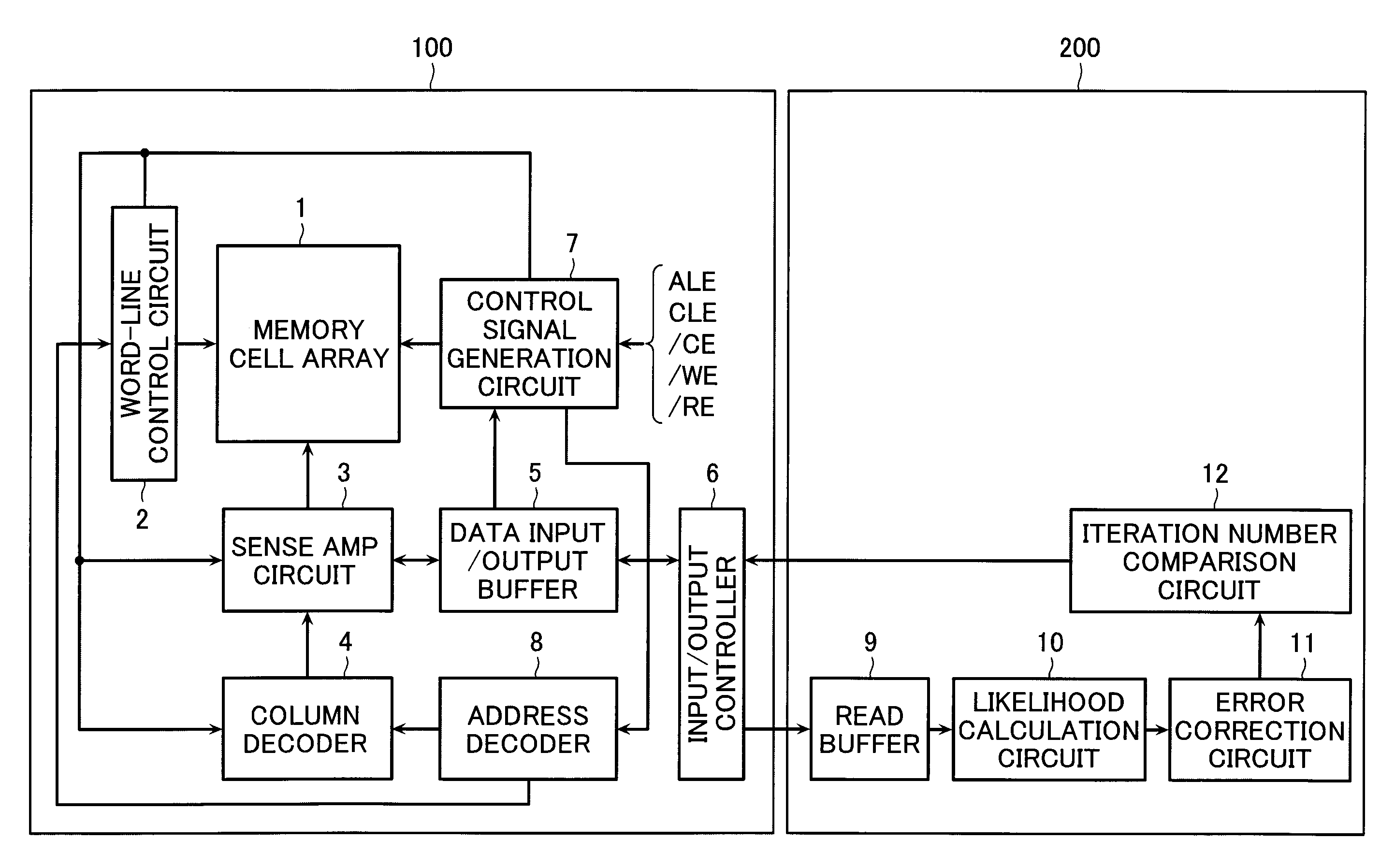
[0137]Next, the second embodiment of the present invention is explained with reference to FIG. 16. Since the same reference numerals are given to the same components as those in the first embodiment, the detailed explanation thereof is omitted hereinbelow.

[0138]This embodiment differs from the first embodiment in that it replaces the iteration number comparator circuit 12 with a likelihood addition circuit 13. The likelihood addition circuit 13 is an example of the refresh control circuit controlling a refresh operation of a memory cell.

[0139]This likelihood addition circuit 13 adds the absolute values of the likelihood values calculated in the likelihood calculation circuit 10. Then, it calculates a sum thereof for every block as a unit of error correction.

[0140]When the sum is smaller than the predetermined reference value, the refresh command is issued for the block in which error correction was conducted (read most recently). It means that the block has a lot of data with a low ...

third embodiment

[0143]Next, the third embodiment of the present invention is explained with reference to FIG. 17. Since the same reference numerals are given to the same components as those in the first embodiment, the detailed explanation thereof is omitted hereinbelow. This embodiment differs from the first embodiment in that it replaces the iteration number comparator circuit 12 with a likelihood comparator / counter circuit 14. This likelihood comparator / counter circuit 14 is an example of the refresh control circuit controlling a refresh operation of a memory cell.

[0144]The likelihood comparator / counter circuit 14 has a function of comparing an absolute value of the likelihood value per input bit with the predetermined reference value, and counting the number of likelihood values smaller than the reference value.

[0145]When the counted result is more than the predetermined reference value, a refresh command is issued for the memory area in which error correction was conducted (read most recently)...

fourth embodiment

[0148]Next, the fourth embodiment of the present invention is explained with reference to FIG. 18. Since the same reference numerals are given to the same components as those in the first embodiment, the detailed explanation thereof is omitted hereinbelow. This embodiment differs from the first embodiment in that it replaces the iteration number comparator circuit 12 with a soft-value comparator / count circuit 15.

[0149]This soft-value comparator / count circuit 15 is an example of the refresh control circuit controlling a refresh operation of a memory cell.

[0150]The soft-value comparator / count circuit 15 has a function of comparing soft-value data per cell input from the read buffer 9 with the predetermined reference value, and counting the number of soft-value data corresponding to the likelihood value with a small absolute value.

[0151]when the number is more than the predetermined reference value, a refresh command is issued for the memory area in which error correction was conducted...


PUM


Abstract

This memory device comprises a word-line control circuit applying a read voltage and a soft-value read voltage as a word line voltage to a word line to generate soft-values. The soft-value read voltage is between an upper limit and a lower limit of each of plural threshold voltage distributions. A likelihood calculation circuit calculates a likelihood value of data stored in a memory cell based on the soft-value. An error correction circuit executes data error correction for the data read from the memory cell based on the likelihood value. A refresh control circuit controls a timing of a refresh operation for the memory cell based on the soft-value or the likelihood value.

Description

CROSS REFERENCE TO RELATED APPLICATIONS[0001]This application is based on and claims the benefit of priority from prior Japanese Patent Application No. 2006-234790, filed on August 31, the entire contents of which are incorporated herein by reference.BACKGROUND OF THE INVENTION[0002]1. Field of the Invention[0003]The present invention relates to a non-volatile semiconductor storage device and a non-volatile semiconductor storage system, and particularly, to a non-volatile semiconductor storage device and a system with a refresh function of memory cells to improve reliability of data.[0004]2. Description of the Related Art[0005]One of the well-known non-volatile semiconductor storage devices is a NAND cell type flash memory. The NAND cell type flash memory includes a memory cell array including a plurality of NAND cell units. Each NAND cell unit includes a plurality of memory cells connected in series and two selection transistors connected to both ends thereof. The memory cell holds...

Claims


Application Information

Patent Timeline
IPC IPC(8): G11C11/34
CPCG11C11/5628G11C11/5642G11C29/00G11C16/3418G11C16/3431G11C16/0483
Inventor ISHIKAWA, TATSUYUKIHONMA, MITSUAKIUCHIKAWA, HIRONORI
Owner KIOXIA CORP
Why Eureka
Try Eureka