Devices with ultrathin structures and method of making same

a technology of ultrathin structures and devices, applied in the direction of fixed capacitor details, fixed capacitors, instruments, etc., can solve the problems of difficulty in further reducing the volume of paste deposited on the substrate, modest incremental improvements, and affecting the thickness of electrodes

Inactive Publication Date: 2008-03-13
NANODYNAMICS INC
View PDF8 Cites 27 Cited by
  • Summary
  • Abstract
  • Description
  • Claims
  • Application Information

AI Technical Summary

Problems solved by technology

Unfortunately, efforts to reduce the thickness of electrodes using the present thick-film technology are hindered by the difficulty of further reducing the volume of paste deposited onto substrates by the screen-printing technique, even when using the finest mesh screens available.
However, these refinements have brought only modest incremental improvements, and the electronic industry is seeking alternative ways to achieve more dramatic reductions in the dimensions of electronic devices and implicitly in the thickness of the metallic layers.
However, the inability of the chemical or physical vapor deposition methods to control directionally the flux of atoms and to obtain sophisticated patterns on a desired substrate without significant metal losses makes them unsuitable for low cost, high throughput mass production of multi-layer structures.
Furthermore, the fully sintered metallic layers deposited by vapor deposition methods may create problems when used in conjunction with “green” ceramic layers, as the subsequent sintering of the latter may generate significant stresses at the metaUceramic interface and affect the structural integrity of complex multi-layer structures.

Method used


Image

  • Devices with ultrathin structures and method of making same
  • Devices with ultrathin structures and method of making same
  • Devices with ultrathin structures and method of making same

Examples


Embodiment Construction

[0026] As used herein and in the appended claims, the singular forms “a,”“an,” and “the” include plural references unless the context clearly dictates otherwise. Thus, for example, reference to “a particle” includes a plurality of such particles, and reference to “the layer” is a reference to one or more layers and equivalents thereof known to those skilled in the art, and so forth. The terms “nanoparticles” and “nanosized particles” are used interchangeably, and refer to particles having a diameter less than about 100 nm. All publications, patent applications, patents, and other references mentioned herein are incorporated by reference in their entirety.

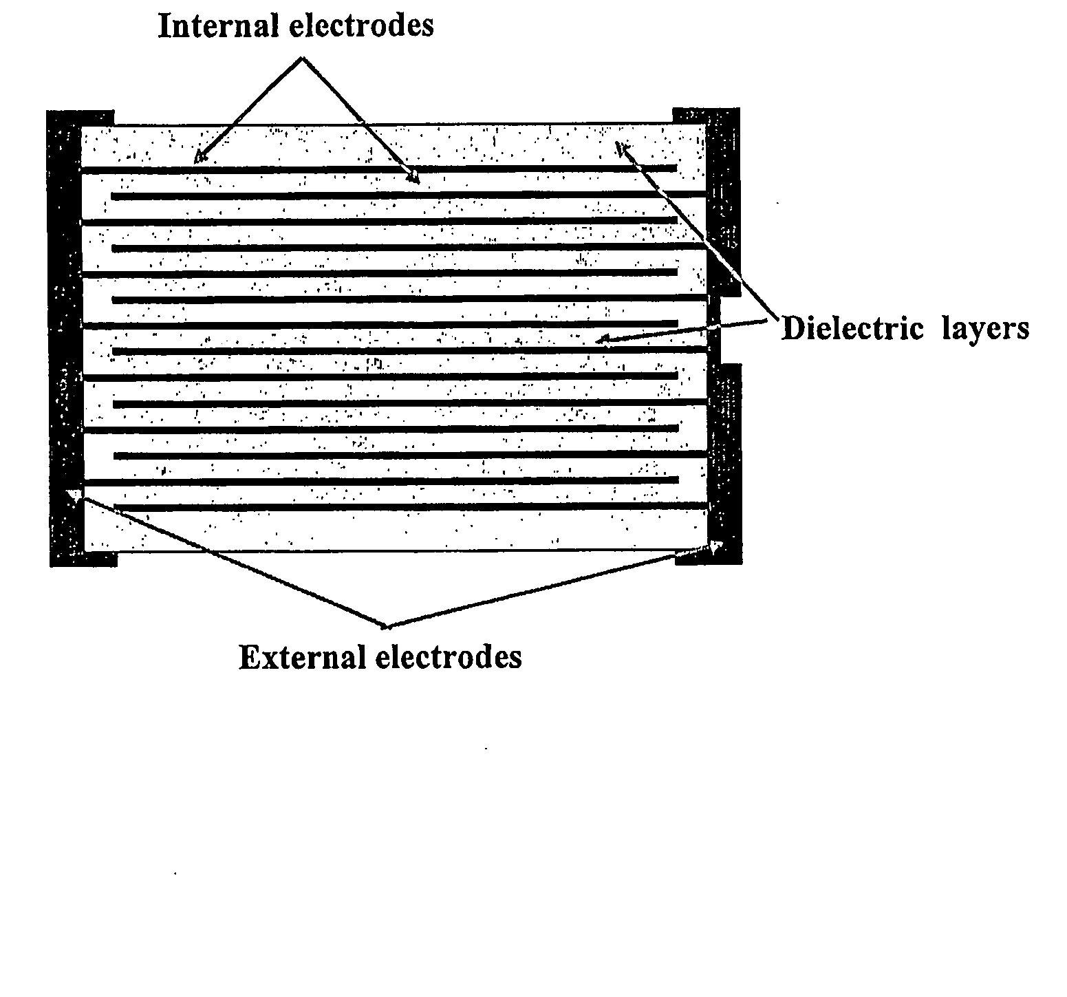
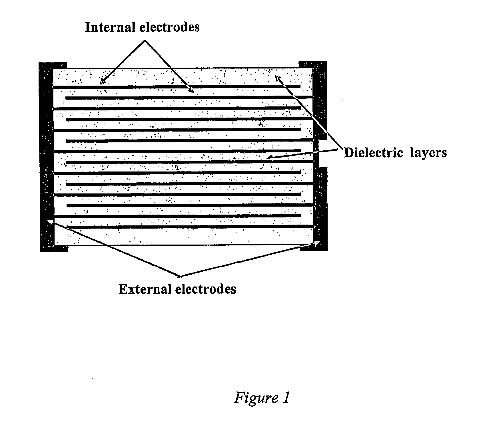
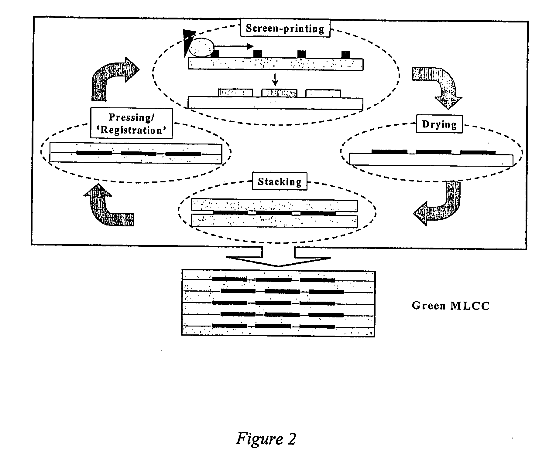
[0027] The present invention provides a method for producing devices having ultrathin structures (e.g., conductive metallic layers), with thickness between about 2 and about 700 nm, and preferably between about 2 and about 200 nm, by depositing a suspension of well-dispersed and uniform nanoparticles onto a substrate, and transform...


PUM

PropertyMeasurementUnit
thicknessaaaaaaaaaa
thicknessaaaaaaaaaa
thicknessaaaaaaaaaa

Abstract

A method of making multilayer electronic devices, such as capacitors and varistors, is provided, wherein nanosized particles are assembled into a densely packed thin film on a dielectric substrate, and then sintered to form an electrode less than about 700 nm in thickness.

Description

RELATED APPLICATIONS [0001] This application is a continuation of PCT International Patent Application Number PCT / US2006 / 009523, filed Mar. 15, 2006, which claims the benefit of U.S. Provisional Application Ser. No. 60 / 661,717, filed Mar. 15, 2005, and the entirety of these applications are hereby incorporated herein by reference for the teachings therein.FIELD OF THE INVENTION [0002] The present invention relates to methods of making electrical devices in general, and capacitors in particular, that feature ultrathin conductive films. BACKGROUND OF THE INVENTION [0003] Metallic particles are used extensively in the electronic industry to construct conductive layers, which may be either intrinsic elements of various components (capacitors, varistors, actuators, etc.) or connecting paths between these components within complex circuits. To a very large extent, these metallic layers are obtained via thick film technology, an approach in which metallic particles are dispersed in high vi...

Claims


Application Information

Patent Timeline
Patent Type & Authority Applications(United States)
IPC IPC(8): H01G4/06B32B5/16
CPCH01C7/18H01C17/283H01G4/0085Y10T428/265Y10T428/26Y10T428/256H01G4/30
Inventor GOIA, DAN V.
Owner NANODYNAMICS INC
Why Eureka
Try Eureka