Eureka AIR delivers breakthrough ideas for toughest innovation challenges, trusted by R&D personnel around the world.

Method of manufacturing nonvolatile memory device

Active Publication Date: 2008-03-13
SK HYNIX INC
View PDF1 Cites 12 Cited by
  • Summary
  • Abstract
  • Description
  • Claims
  • Application Information

AI Technical Summary

Benefits of technology

[0010]An embodiment of the present invention is directed to a method of manufacturing a nonvolatile memory device, which method can overcome the interference phenomenon between neighboring word lines by reducing(for example, by an amount of at least about a half) the opposing area between floating gates in neighboring word lines by changing the shape of the floating gates.

Problems solved by technology

The interference phenomenon becomes substantial due to the interference capacitance, making normal cell operation difficult.

Method used


Image

  • Method of manufacturing nonvolatile memory device
  • Method of manufacturing nonvolatile memory device
  • Method of manufacturing nonvolatile memory device

Examples


Embodiment Construction

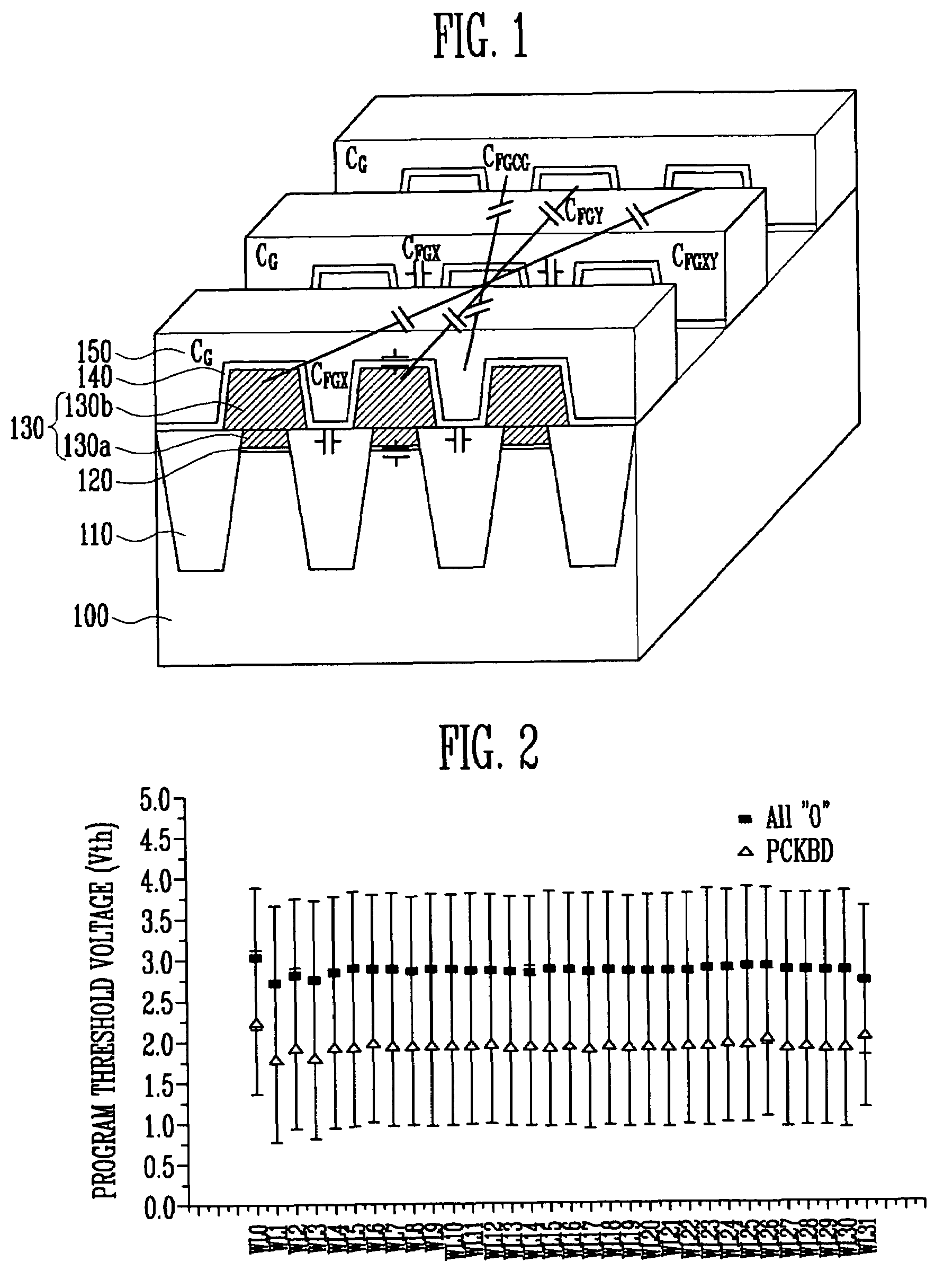
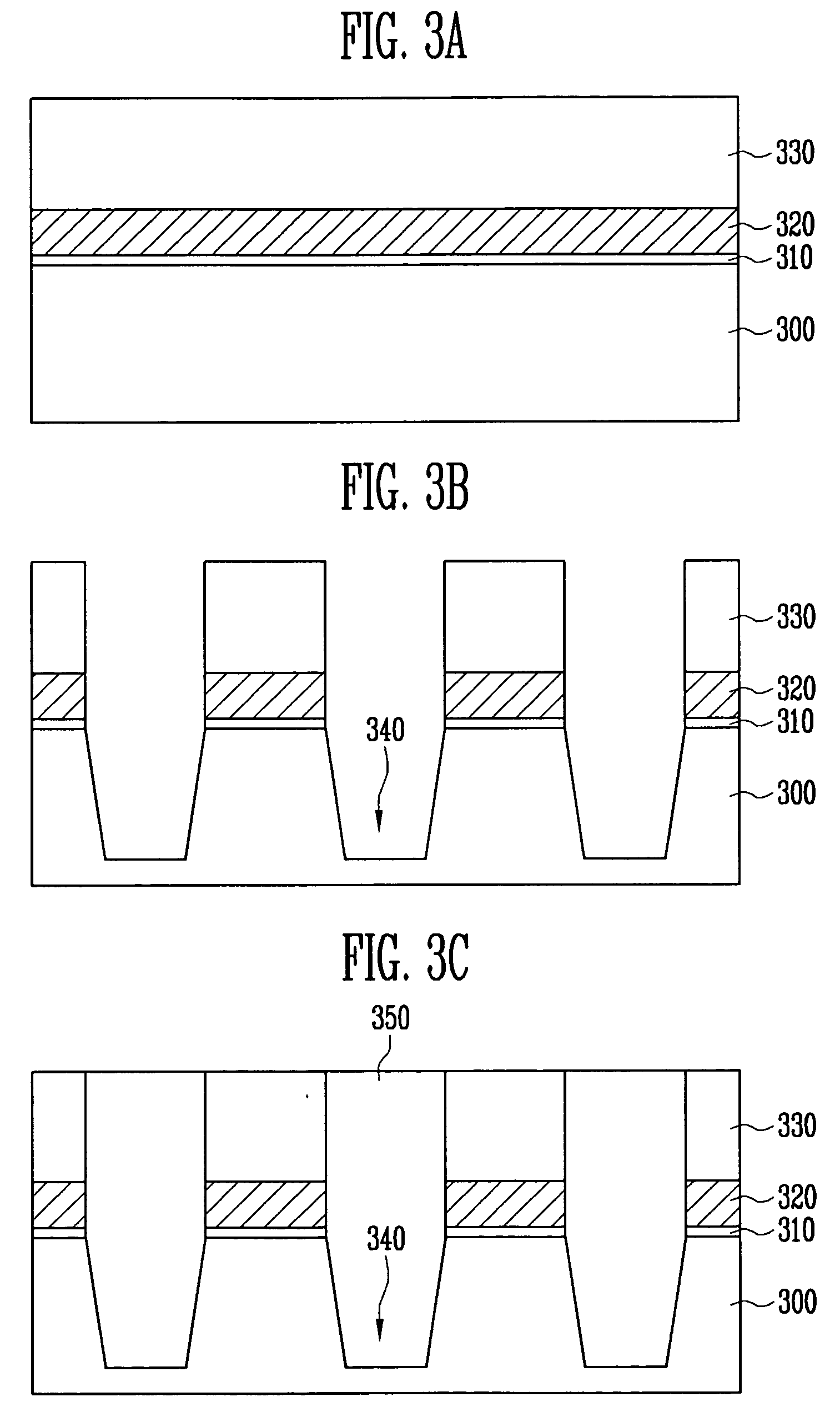
[0015]Specific embodiments according to the present disclosure are described with reference to the accompanying drawings.

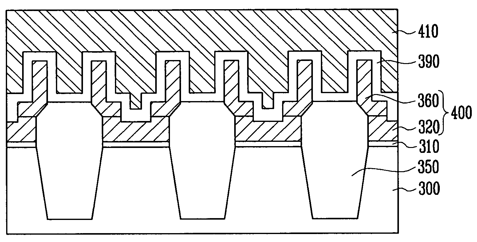
[0016]Referring to FIG. 3A, a tunnel oxide layer 310, a first conductive layer 320 for a floating gate, and a hard mask layer 330 are sequentially formed over a semiconductor substrate 300.

[0017]The tunnel oxide layer 310 can be formed from silicon oxide (SiO2) using an oxidation process.

[0018]The first conductive layer 320 can be formed from a polysilicon layer or a metal layer. Preferably, the first conductive layer 320 is formed using a polysilicon layer with a good surface adhesive property. Furthermore, the first conductive layer 320 can be formed by chemical vapor deposition (CVD) or physical vapor deposition (PVD), preferably by low pressure CVD (LPCVD).

[0019]The hard mask layer 330 is formed from a material with an etch selectivity different from that of the first conductive layer 320. Preferably, the hard mask layer 330 is formed from a nitride-based mate...


PUM


Abstract

A method of manufacturing a nonvolatile memory device is disclosed. The method includes the steps of forming a tunnel oxide layer, a first conductive layer for a floating gate, and a hard mask layer over a semiconductor substrate, etching a portion of the hard mask layer, the first conductive layer, the tunnel oxide layer and the semiconductor substrate, forming trenches, gap-filling the trenches with an insulating material to form isolation layers, removing the hard mask layer, forming second conductive layer for a floating gate on the entire surface, forming spacers on vertical faces of the second conductive layer, removing the second conductive layer on the isolation layers and between the spacers by means of an etch process using the spacers as etch masks, removing the spacers, and forming a dielectric layer and a third conductive layer on the entire surface including the second conductive layer. The method reduces the interference capacitance between neighboring word lines, minimizes the interference phenomenon, and minimizes the distributions of the program threshold voltage Vth between word lines.

Description

BACKGROUND OF THE INVENTION[0001]The present invention relates to nonvolatile memory devices and, more particularly, to a method of manufacturing a nonvolatile memory device, which method can reduce the interference capacitance between neighboring word lines.[0002]Information stored in the cells of a nonvolatile memory device is not lost when the power is off. The nonvolatile memory device includes a thin tunnel oxide layer, a floating gate, a control gate, and an insulator for isolating the two gates, which are formed over a silicon substrate.[0003]FIG. 1 is a perspective view of a conventional NAND flash memory device.[0004]Referring to FIG. 1, isolation layers 110 are formed by a Shallow Trench Isolation (STI) process, and define a field region and an active region. A tunnel oxide layer 120 is formed over a semiconductor substrate 100 in which the isolation layers 110 are formed. Floating gates 130 are formed on the tunnel oxide layer 120 to overlap with the edges of the isolatio...

Claims


Application Information

Patent Timeline
IPC IPC(8): H01L21/336
CPCH01L21/28273H01L27/115H01L29/7881H01L29/42324H01L27/11521H01L29/40114H10B69/00H10B41/30H01L21/31144H01L21/76224
Inventor DONG, CHA DEOK
Owner SK HYNIX INC
Why Eureka
Eureka Blog
Learn More