Driving circuit and data driver of planar display device

Inactive Publication Date: 2008-03-20
RENESAS ELECTRONICS CORP
View PDF4 Cites 13 Cited by
  • Summary
  • Abstract
  • Description
  • Claims
  • Application Information

AI Technical Summary

Benefits of technology

[0013]The data driver of the planar display device of the present invention includes: a shift register for generating a shift pulse in synchronization with a clock signal in response to a start signal; a data register for sequentially fetching data signal in synchronization with the shift pulse; and a data latch circuit for latching the data signal fetched into the data register. This data driver is characterized in that the timing of the latch can be controlled.
[0014]According to the present invention, in each of the plural data drivers, the timing of the internal latch signal can be independently controlled and the timing of the latch operation can be shifted between the plural data drivers. With this invention, the source current of the driver circuit, which flows through the power-supply lines of the device, can be generated in a different time for each driver circuit, and a peak value of the source current is suppressed low so as to minimize the intensity of generating the EMI. At the same time, its time difference is controlled by a frequency of an integral multiplication of a cycle of the clock signal so as to avoid having the resonance frequency of the display device, and thereby the generation of the EMI of the display device can be suppressed.

Problems solved by technology

When the above-mentioned latch operations are simultaneously performed by the data drivers under such a circumstance, currents relating to the latch operations of all the data drivers simultaneously flow to a power-supply line common in the display device, which results in increasing electro-magnetic interference (hereinafter referred to as “EMI”).
This delay time varies for each product driver circuit depending on manufacturing conditions, and its control is not easy.
In addition, even in the same product driver circuits, this delay time varies depending on a temperature of the environment and a source voltage, and its control is also not easy.
However, by the technology disclosed in Japanese Patent Application Laid-open publication No. 8-22268, its control is not easy because of the above-described reason.
As a result, there is a disadvantage in that the EMI of the display device cannot be prevented from occurring depending on the combination of the device and the driver circuit mounted thereon or the usage environment.

Method used


Image

  • Driving circuit and data driver of planar display device
  • Driving circuit and data driver of planar display device
  • Driving circuit and data driver of planar display device

Examples


Embodiment Construction

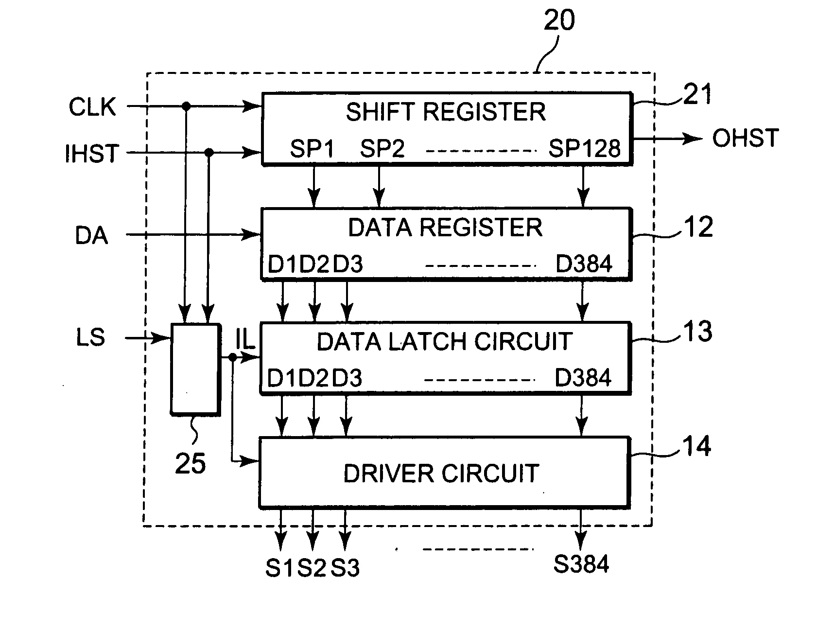
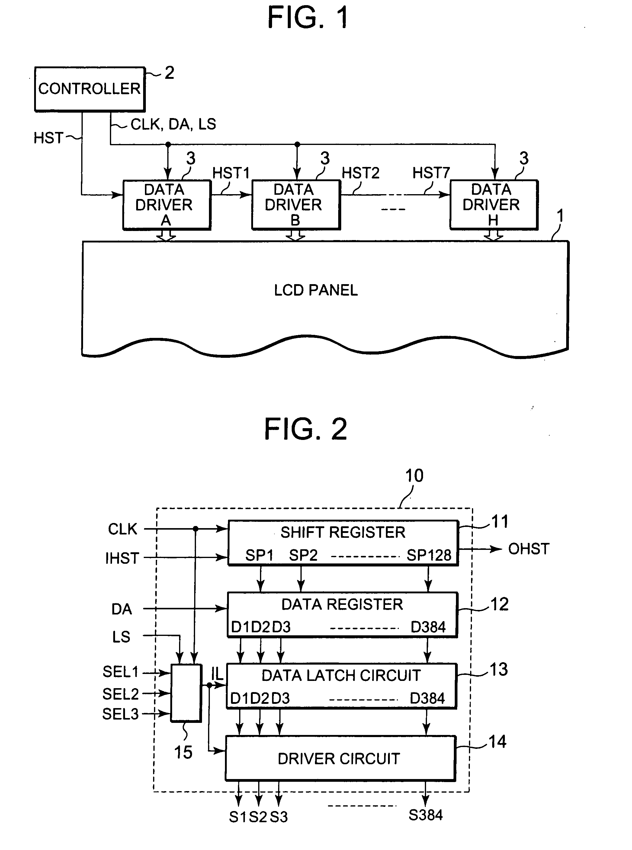
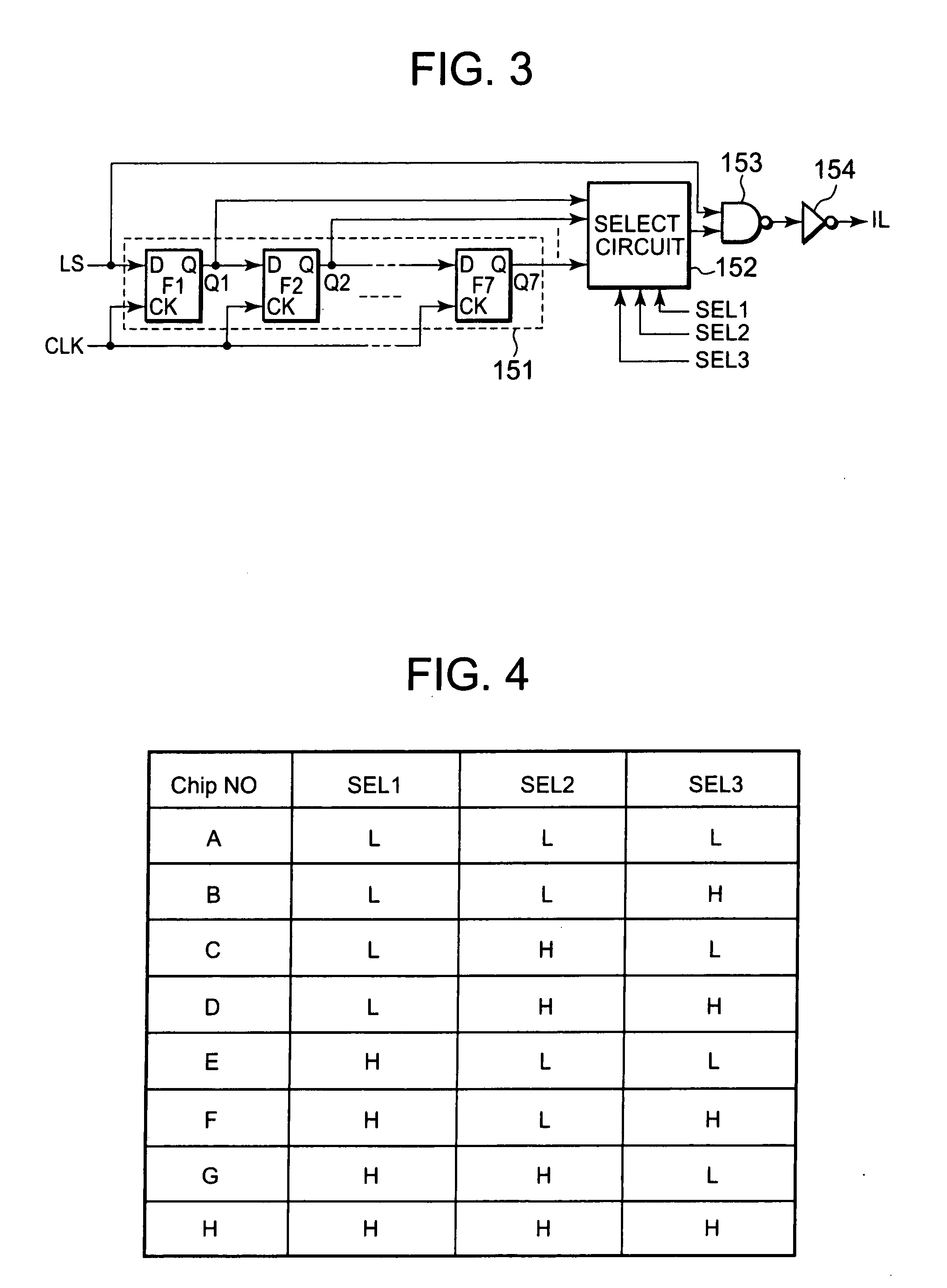
[0024]With reference to drawings, an embodiment of the present invention will be described below. FIG. 1 shows one embodiment of the present invention. A driving circuit of a liquid crystal panel 1 is provided with a controller 2 and data drivers 3. For example, eight of the data drivers 3 (A, B . . . , and H) are arranged by taking the case as an example where the liquid crystal panel 1 has a resolution of XGA (1024×768 pixels: one pixel is formed of three dots of R (red), G (green), and B (blue)) and each of the data drivers covers displaying 128 pixels (outputs 128×3 dots=384 outputs).

[0025]In each of the eight data drivers 3, a start signal HST is supplied from the controller 2 to a first-stage data driver A. The eight data drivers 3 are cascade-connected by cascade outputs HST1, HST2, . . . , HST7 from each of the data drivers 3. In addition, a clock signal CLK, a data signal DA, and a latch signal LS are commonly supplied from the controller 2 to each of the data drivers 3.

[00...


PUM


Abstract

A clock signal, a data signal, and a latch signal are commonly supplied from a controller to a plurality of the data drivers. The data signal and the latch signal are synchronized with the clock signal. In each of the data drivers, an internal latch signal is generated in synchronization with the clock signal in response to the latch signal. Timing of a rising edge of the internal latch signal is independently controlled in each data driver in accordance with position information where each data driver is arranged.

Description

BACKGROUND OF THE INVENTION[0001]1. Field of the Invention[0002]The present invention relates to a driving circuit and data driver of a planar display device.[0003]2. Description of Related Art[0004]As a dot matrix display device, a liquid crystal display device has been used for various types of devices such as a personal computer because it has characteristics of thin, light, and low-power consumption. In particular, an active matrix color liquid crystal display device, which has an advantage in controlling high definition image quality, has been the mainstream of it.[0005]A liquid crystal display module of this type of liquid crystal display device includes: a liquid crystal panel (LCD panel); a control circuit (hereinafter referred to as a controller) formed of a semiconductor integrated circuit device (hereinafter referred to as an IC); a scanning-side driving circuit (hereinafter referred to as a scanning driver) formed of the IC; and a data-side driving circuit (hereinafter r...

Claims


Application Information

Patent Timeline
IPC IPC(8): G06F3/038
CPCG09G3/3688G09G2330/06G09G2310/0286
Inventor FUKUO, MOTOO
Owner RENESAS ELECTRONICS CORP
Why Eureka
Try Eureka