Semiconductor Light Emitting Device

a semiconductor and light-emitting technology, applied in the direction of semiconductor devices, basic electric elements, electrical appliances, etc., can solve the problems of insufficient flow current effective in the entire device, insufficient light-emitting efficiency, and insufficient use of current diffusion layers as transparent current diffusion layers, etc., to achieve a large light-emitting output and superior light-emitting efficiency

Inactive Publication Date: 2008-03-27
ROHM CO LTD
View PDF2 Cites 25 Cited by
  • Summary
  • Abstract
  • Description
  • Claims
  • Application Information

AI Technical Summary

Benefits of technology

[0051] As described above, according to the present invention, because the GaN-based semiconductor light emitting device can take out light effectively from the top surface and side faces of the transparent electrode layer and the insulating layer by depositing the transparent electrode layer or the insulating layer to an optimum thickness, a semiconductor light emitting device can be obtained that is superior in light emitting efficiency and that has a large light emitting output.

Problems solved by technology

On the other hand, in a LED made of a GaN-based material (GaN-based LED) that emits green, blue, purple, or ultraviolet light, there is a problem that the above-described materials are opaque to a light emission wavelength (a wavelength of the light emitted in the light emitting layer, below the same) and are not appropriate as a transparent current diffusion layer.
However, the p-type GaN-based semiconductor layer is not preferable because the thickness is normally 0.3 μm or less due to its high resistance and element resistance increases by thickening further.
Therefore, it is not appropriate to use as the current diffusion layer flowing current effectively in the entire device.
However, light extraction efficiency is poor.
However, under the present conditions, it is inferior to the light emitting efficiency of a luminescent lamp, and technology that further increases the light emitting efficiency of the GaN-based LED for practical use is necessary.
However, it becomes difficult to radiate to the outside of the element (which means semiconductor layers and electrodes of one chip, below the same), in case of lights which transmits to the direction tilted from the vertical direction, though they are most of the light emitted in the light emitting layer, they may be captured in the inside of the element by repeating total reflections in the element, and there is a problem that it is not radiated to the outside of the element.

Method used


Image

  • Semiconductor Light Emitting Device
  • Semiconductor Light Emitting Device
  • Semiconductor Light Emitting Device

Examples


first embodiment

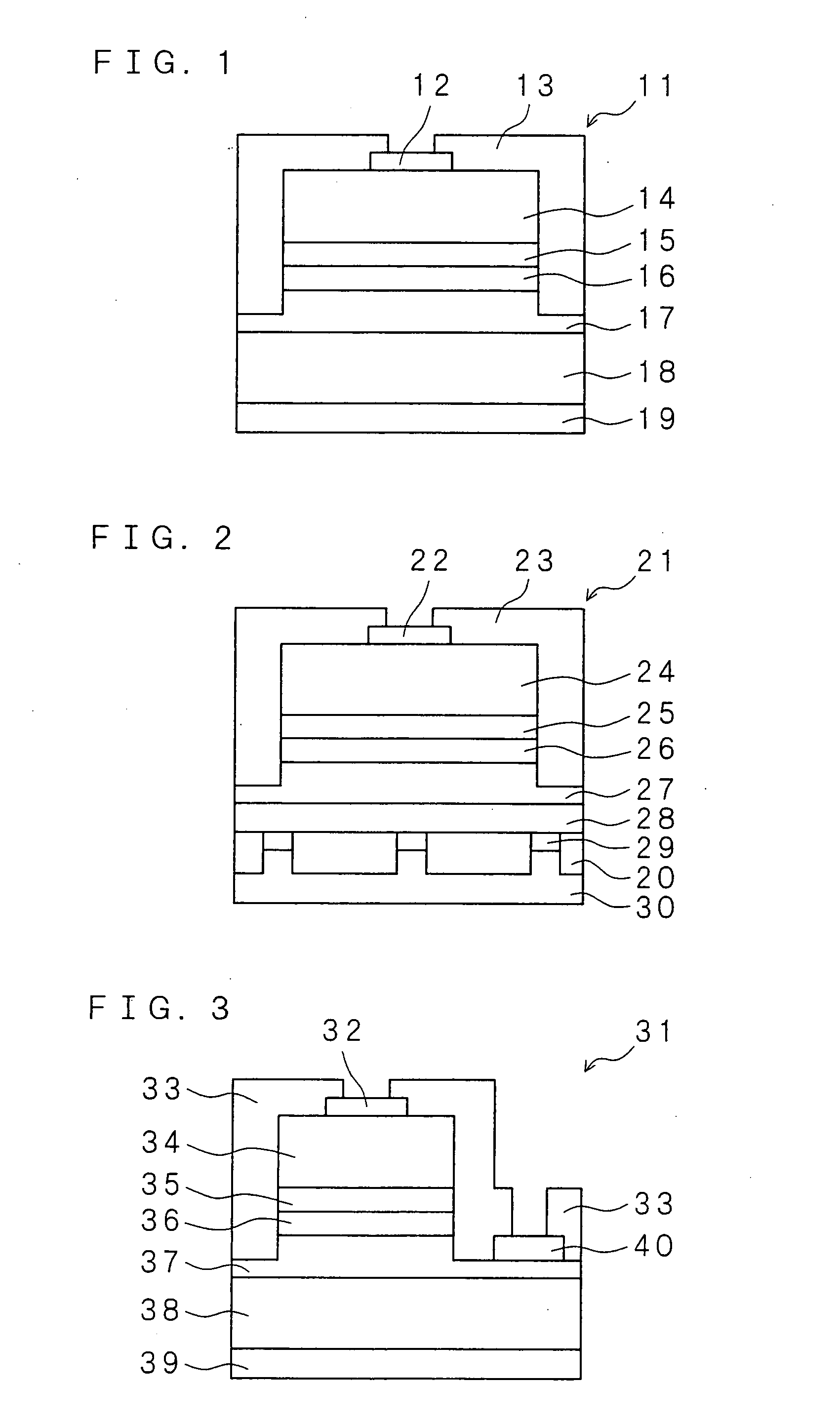
[0078] Below, the embodiments of the present invention are explained referring to the attached Figures. the present invention is shown in FIG. 1. As shown in FIG. 1, a light emitting device (semiconductor light emitting device) 11, which is a GaN-based semiconductor light emitting device, includes a metal electrode 12, an insulating layer 13, a transparent electrode layer 14, a p-type GaN-based semiconductor layer 15, a GaN-based semiconductor light emitting layer 16, an n-typed GaN-based semiconductor layer 17, a conductive substrate 18, and a second metal electrode layer 19. The second metal electrode layer 19 of the present embodiment may function as a reflection electrode layer.

[0079] Such the GaN-based semiconductor light emitting device is preferably formed using a metal organic chemical vapor deposition method (MOCVD), and other than this, a molecular beam epitaxy method (MBE), an HVPE method, etc. are also preferable. First, using these methods, the n-type GaN-based semicond...

second embodiment

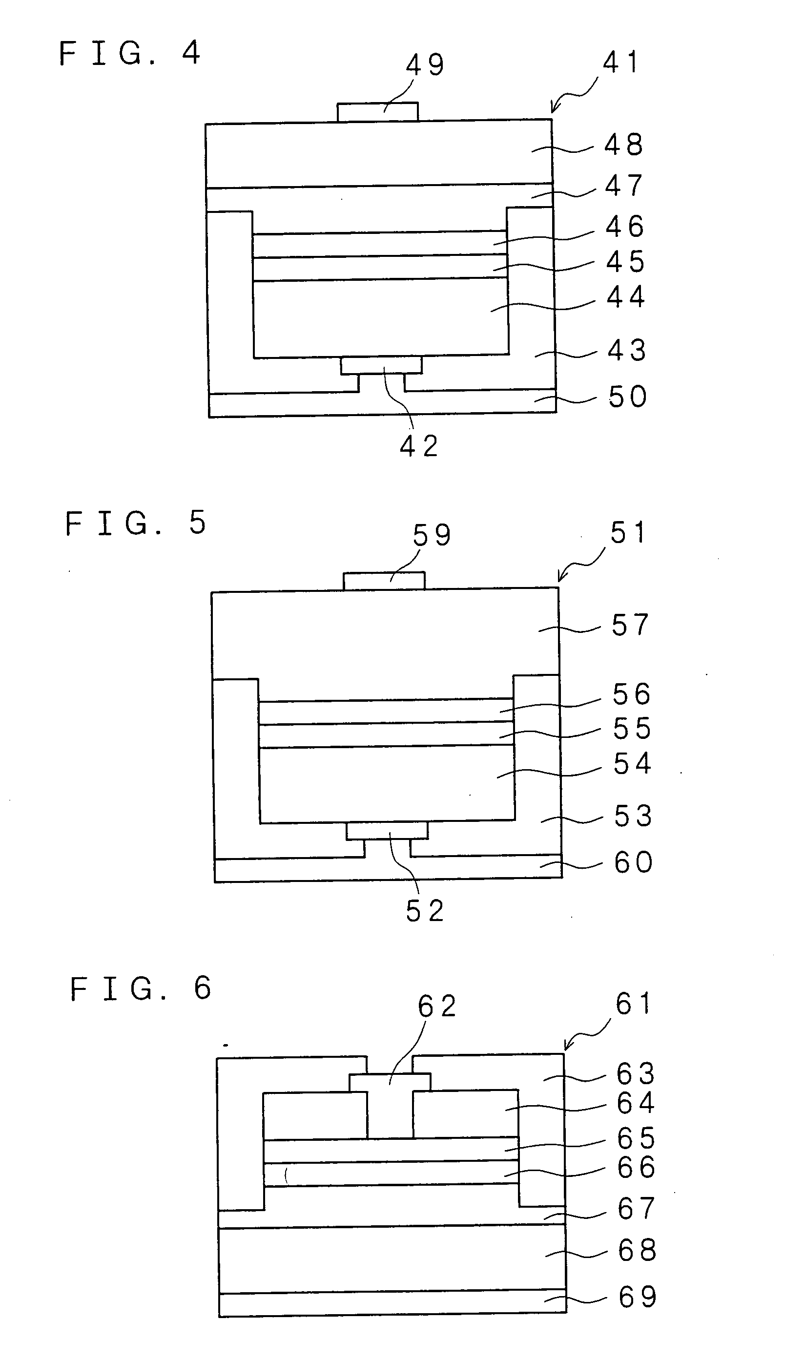
[0094] The second embodiment in the present invention is shown in FIG. 2. As shown in FIG. 2, a light emitting device (semiconductor light emitting device) 21 includes a metal electrode 22, an insulating layer 23, a transparent electrode layer 24, a p-type GaN-based semiconductor layer 25, a GaN-based semiconductor light emitting layer 26, an n-type GaN-based semiconductor layer 27, a conductive substrate 28, a pattern electrode layer 29, a second insulating layer 20, and a reflection electrode layer 30.

[0095] The difference with the first embodiment is a point that the pattern electrode layer 29, the second insulating layer 20, and the reflection electrode layer 30 are formed in order to improve a reflectivity on the back surface side of the conductive substrate.

[0096] The formation of the light emitting device 21 in the second embodiment has the same manufacturing steps as the formation of the metal electrode 12 on the transparent electrode layer 14 in the first embodiment up to ...

third embodiment

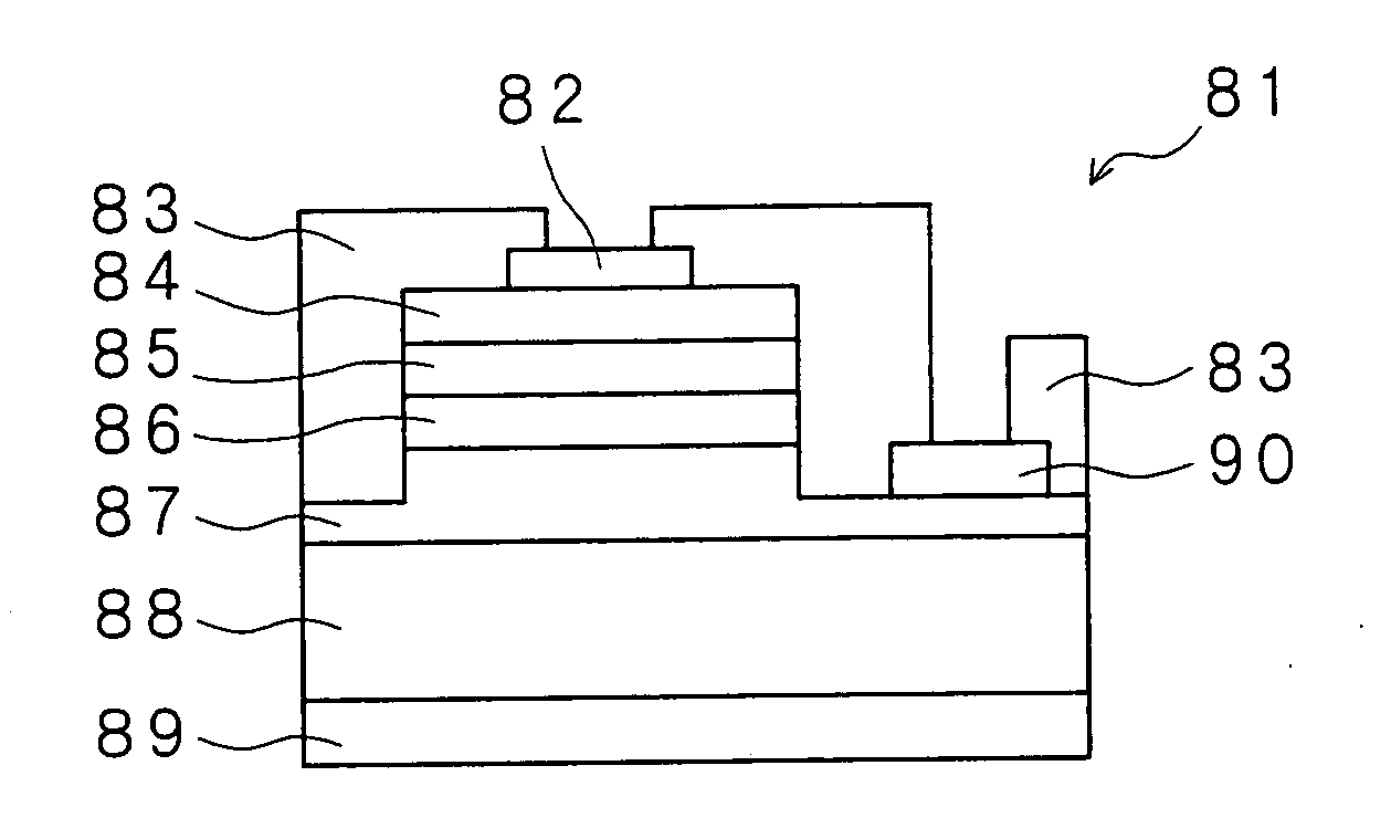
[0100] The third embodiment in the present invention is shown in FIG. 3. As shown in FIG. 3, a light emitting device (semiconductor light emitting device) 31 includes a metal electrode 32, an insulating layer 33, a transparent electrode layer 34, a p-type GaN-based semiconductor layer 35, a GaN-based semiconductor light emitting layer 36, an n-type GaN-based semiconductor layer 37, a non-conductive substrate (insulating substrate) 38, a reflection metal layer 39, and a second metal electrode 40.

[0101] The difference with the first embodiment is a point that the substrate 38 is non-conductive and that due to it, the second metal electrode 40 is formed on a part of an exposed surface of the n-type GaN-based semiconductor 37 and the reflection metal layer 39 is formed on the back surface of the non-conductive substrate 38. Sapphire (Al2O3) is preferable for the non-conductive substrate 38.

[0102] In order to form the light emitting device 31 in the third embodiment, the manufacturing s...


PUM


Abstract

A semiconductor light emitting device is provided, in which the light emitting efficiency of a LED is improved. A semiconductor light emitting device (11) includes a light emitting layer (16) made of a GaN-based semiconductor sandwiched with an n-type GaN-based semiconductor layer (17) and a p-type GaN-based semiconductor layer (15), and a ZnO-based or an ITO transparent electrode layer (14). Further, a value of an equation represented by 3t/(A/π)1/2−3(t/(A/π)1/2)2+(t/(A/π)1/2)3 is 0.1 or more, where a thickness of the transparent electrode layer is represented by t and an area of the light emitting layer (light emitting area) of the light emitting device (11) is represented by A. The light emitting efficiency is improved using the transparent electrode layer (14) having an optimum thickness to the light emitting area.

Description

FIELD OF THE INVENTION [0001] The present invention relates to a GaN-based semiconductor light emitting device formed with GaN-based semiconductor layers. Especially, it relates to a GaN-based semiconductor light emitting device superior in light emitting efficiency and light emitting output. BACKGROUND OF THE INVENTION [0002] The GaN-based semiconductor light emitting device comprising the GaN-based semiconductor layer is considered to be a next generation lighting source replacing the fluorescent lamp. The GaN-based semiconductor light emitting device basically includes a pn junction diode in which a light-emitting layer is sandwiched between an n-type GaN-based semiconductor layer and a p-type GaN-based semiconductor layer. Electrons are injected into the light emitting layer from the n-type GaN-based semiconductor layer, holes are injected into the light emitting layer from the p-type GaN-based semiconductor layer, and they are recombined and emit light in the light emitting lay...

Claims


Application Information

Patent Timeline
Patent Type & Authority Applications(United States)
IPC IPC(8): H01L33/00H01L33/32H01L33/40H01L33/42
CPCH01L33/32H01L33/42H01L33/405
Inventor TAMURA, KENTARONAKAHARA, KEN
Owner ROHM CO LTD
Why Eureka
Try Eureka