

Semiconductor integrated circuit
- Summary
- Abstract
- Description
- Claims
- Application Information
AI Technical Summary
Benefits of technology
Problems solved by technology
Method used
Image

Examples
first embodiment
(1) First Embodiment
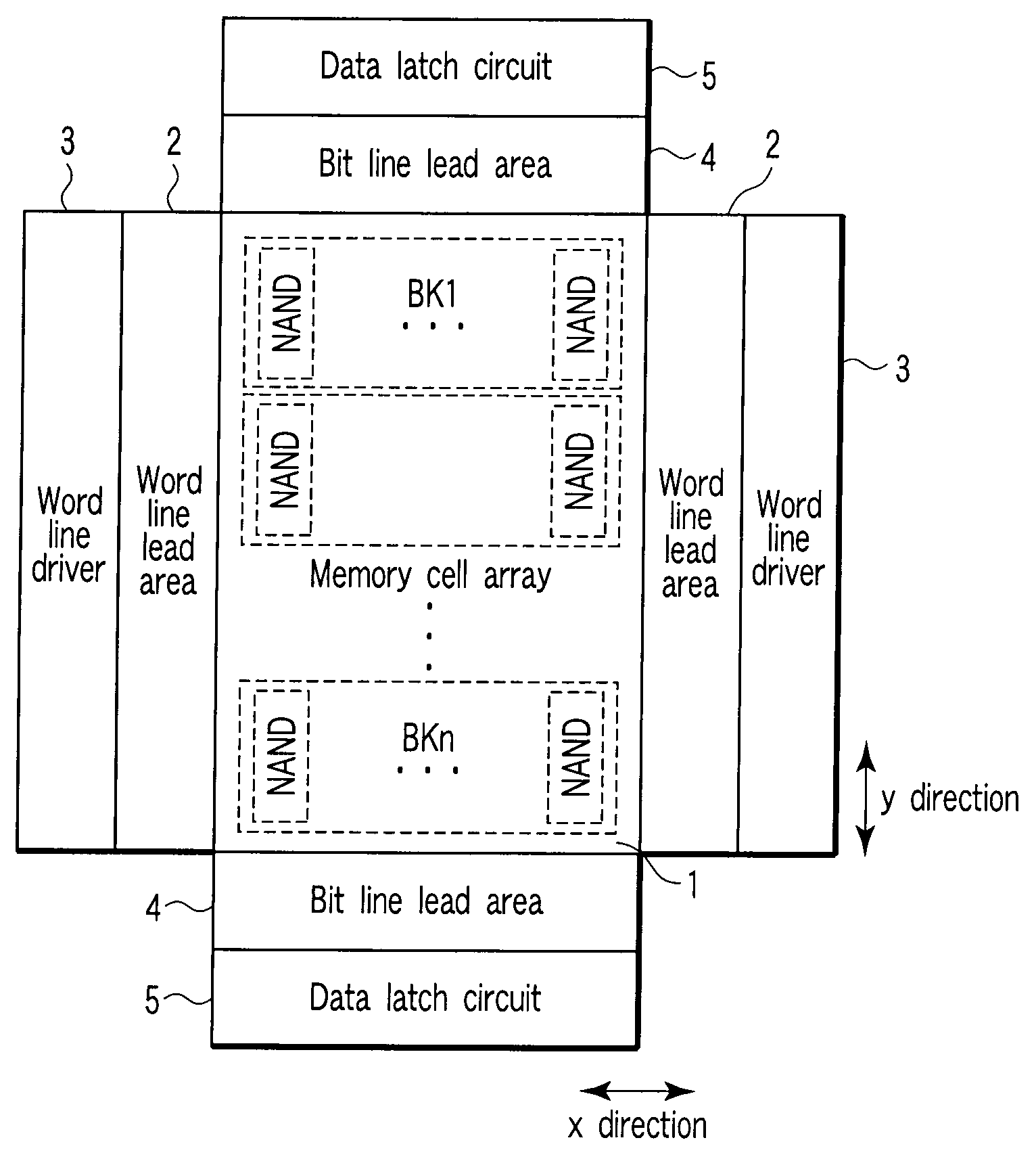
[0033]FIG. 1 is a schematic diagram showing the configuration of a flash memory for explaining the embodiments of the present invention. It is to be noted that FIG. 1 shows the configuration of a NAND type flash memory.
[0034]A memory cell array section 1 is constituted of a plurality of blocks BK1, BK2, . . . , BKn. Each of the plurality of blocks BK1 to BKn has a plurality of NAND cell units.
[0035]A word line driver 3 drives word lines in the block selected during read / write.
[0036]A data latch circuit 5 has a function of temporarily latching data during read / write.
[0037]Furthermore, a word line lead area 2 is provided between a memory cell array 1 and the word line driver 3 as a region for connecting lead wires to the word lines, and a bit line lead area 4 is provided between the memory cell array 1 and the data latch circuit 5 as a region for connecting the lead wires to bit lines. The word line lead areas 2 have the memory cell array 1 in between, and are arra...
second embodiment
(2) Second Embodiment
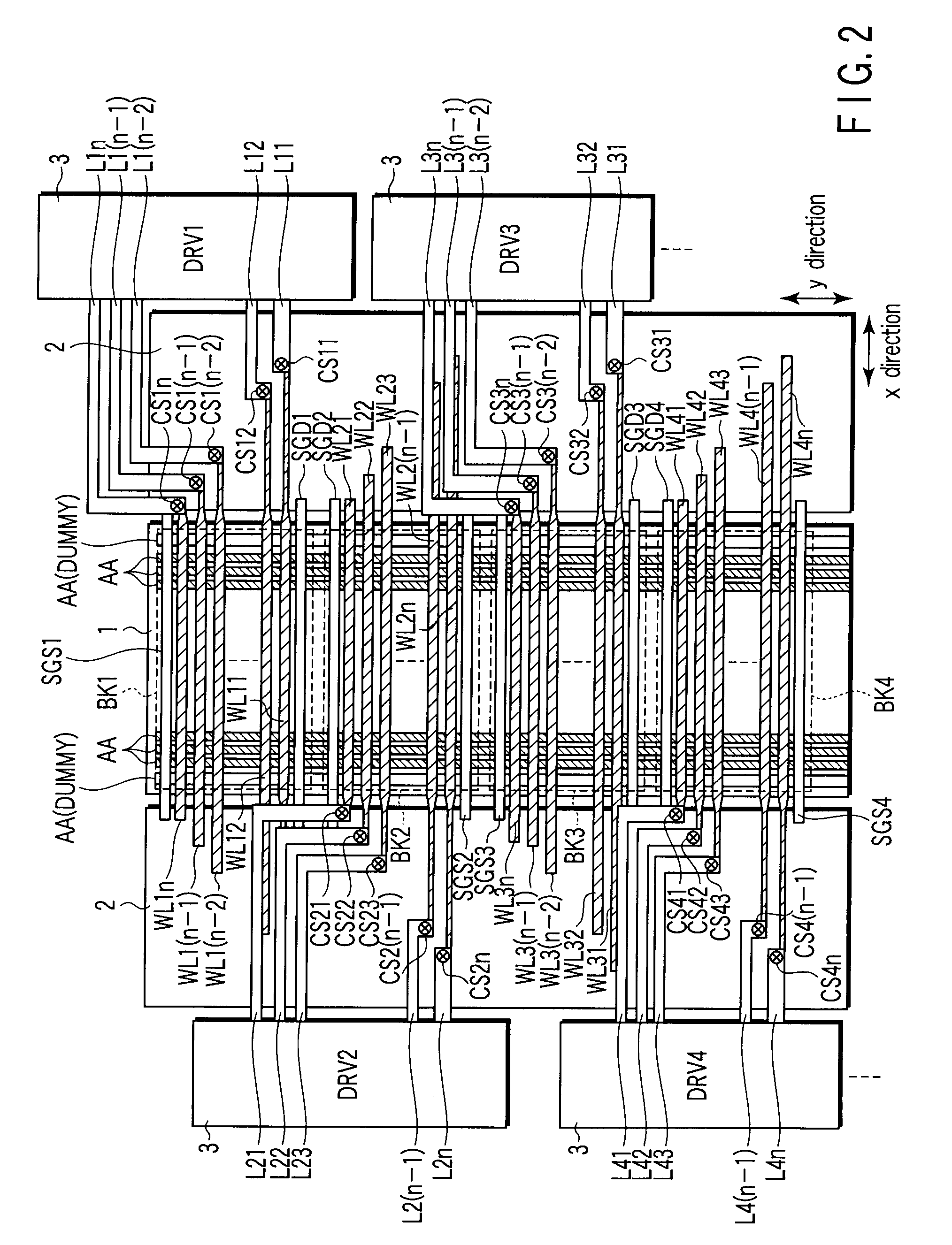
[0071]A second embodiment will be described using FIGS. 6 to 8. It is to be noted that the same signs are assigned to the same members as those in FIGS. 2 to 5 and these members are not described in detail.
[0072]As shown in FIGS. 6 to 8, a plurality of word lines WL11 to WL1n have a single-edged shape at one end and the other in word line lead areas 2 as in the first embodiment.
[0073]In the present embodiment as well, a block BK1 shown in FIG. 6 is explained below as an example as in the first embodiment.
[0074]A plurality of contact holes CS11 to CS1n are disposed at one end of the plurality of word lines WL11 to WL1n.
[0075]The width of the plurality of word lines WL11 to WL1n in the word line lead area 2 where the plurality of contact holes CS11 to CS1n are disposed is smaller than the width of the plurality of word lines WL11 to WL1n in a memory cell array 1.
[0076]Furthermore, the other end of the plurality of word lines WL11 to WL1n is disposed in the word l...
PUM
 Abstract
Description
Claims
Application Information