Semiconductor integrated circuit device

a technology of integrated circuit device and semiconductor, which is applied in the direction of semiconductor device details, semiconductor/solid-state device details, diodes, etc., can solve the problems of occupying more area of esd protection circuit, not achieving the protection performance required of a protection diode, e.g. current-carrying capacity, etc., and achieves appropriate protection performance and reduces the effect of area

Inactive Publication Date: 2008-03-27
LAPIS SEMICON CO LTD
View PDF3 Cites 27 Cited by
  • Summary
  • Abstract
  • Description
  • Claims
  • Application Information

AI Technical Summary

Benefits of technology

[0010]The protection diode is formed by providing the anode region that faces the guard ring region on the semiconductor substrate and by using the guard ring region as th

Problems solved by technology

This causes the ESD protection circuit to occupy more area than the output transistor.
This prevents the semiconductor integrated circuit device from operating normally, and results in damage of the integrated circuit device.
The use of this PNP

Method used


Image

  • Semiconductor integrated circuit device
  • Semiconductor integrated circuit device
  • Semiconductor integrated circuit device

Examples


first embodiment

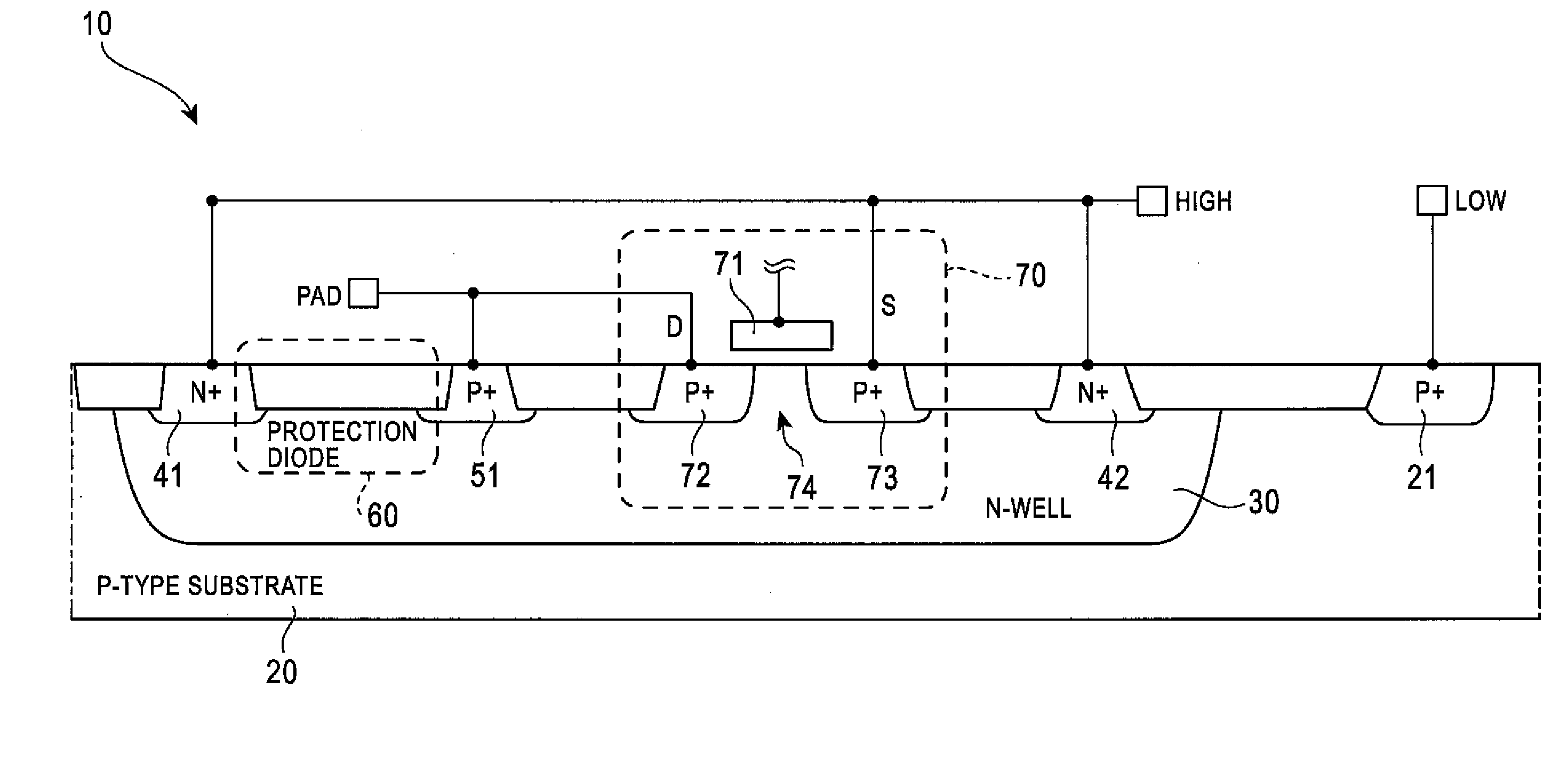
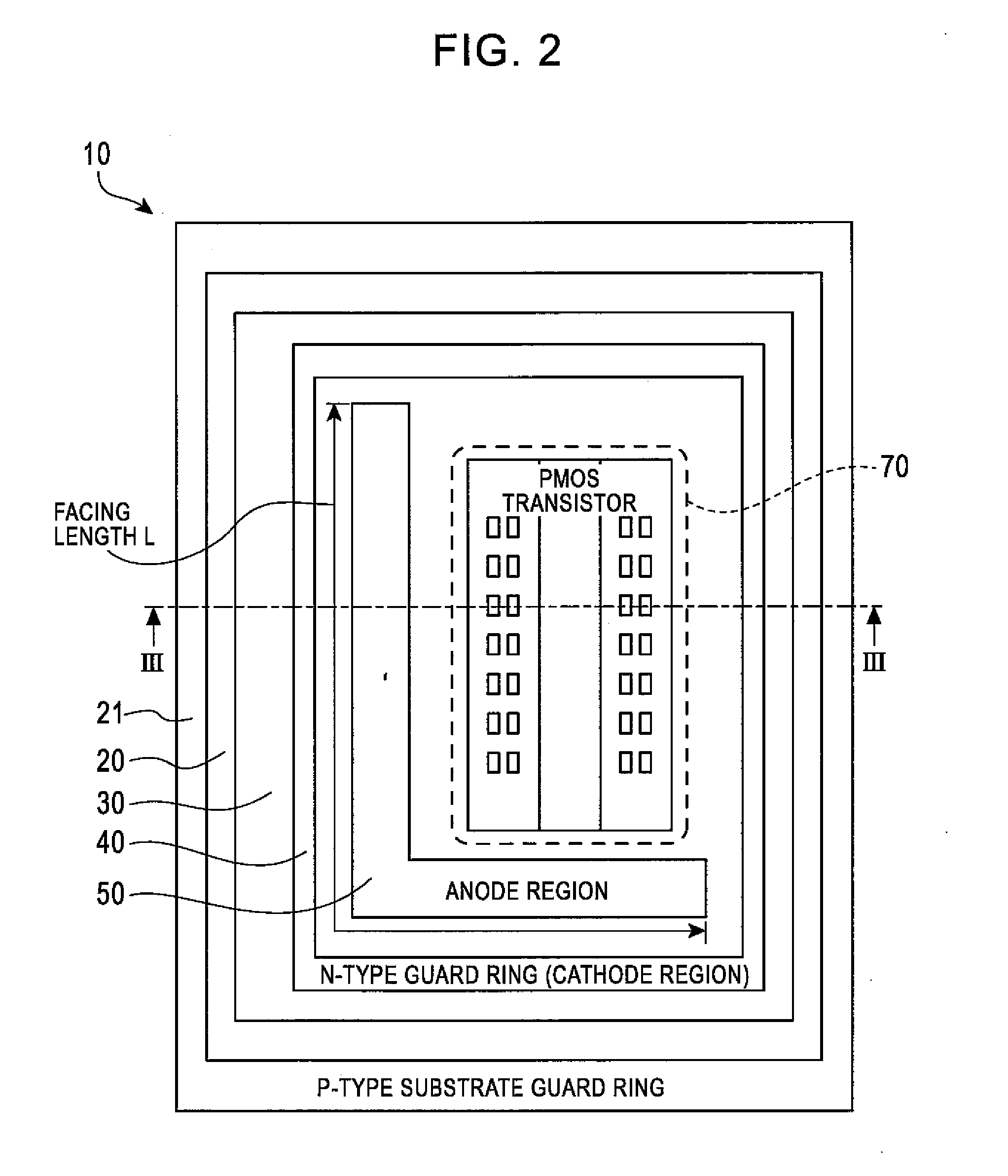
[0017]Referring to FIG. 2, the first embodiment of the semiconductor integrated circuit device 10 according to the present invention will be described. The semiconductor integrated circuit device 10 constitutes a so-called LSI (a large-scale integrated) circuit. A large number of semiconductor elements, such as PMOS transistors and NMOS transistors for achieving a variety of functions, are formed on a P-type substrate 20. In particular, a PMOS transistor 70 is formed, as an output transistor that is shown in the drawing, on the P-type substrate 20, with an n-well 30 interposed therebetween. The PMOS transistor 70 is assumed to be electrically connected to the outside through an output terminal, requiring ESD protection countermeasures.

[0018]The n-well 30 is the main region of the circuit device 10 and has an N type conductivity. In this embodiment, one conductivity type (first conductivity type) is an N type and the other (or second) conductivity type is a P type.

[0019]An N-type gua...

second embodiment

[0028]Referring to FIG. 5, a second embodiment of the semiconductor integrated circuit device 10 according to the present invention will be described. Similar reference numerals and symbols are used in the first and second embodiments to designate similar elements. In the semiconductor integrated circuit device 10, a PMOS transistor 70 is formed, as an output transistor, on a P-type substrate 20 with an n-well 30 interposed therebetween, in the same manner as in the first embodiment. The PMOS transistor 70 is assumed to be electrically connected to the outside through an output terminal. This requires ESD protection countermeasures.

[0029]An N-type guard ring 40 is formed on the n-well 30 so as to surround the PMOS transistor 70. A P-type substrate guard ring 21 is formed on the P-type substrate 20 so as to surround the N-type guard ring 40. An anode region 50, which is one of the most important elements of the present invention, is formed between the PMOS transistor 70 and the N-typ...


PUM


Abstract

A semiconductor integrated circuit device includes at least one MOS transistor that is formed in a main region of the circuit device. The main region has one conductivity type. The semiconductor integrated circuit device also includes a guard ring region formed surrounding the MOS transistor and in contact with the main region. The guard ring has the same conductivity type as the main region. The semiconductor integrated circuit device further includes an anode region formed facing the guard ring region and in contact with the main region. The anode region has the opposite conductivity type to the main region. The semiconductor integrated circuit device also includes a cathode region having at least a portion of the guard ring region. The anode region, the main region, and the cathode region form a diode.

Description

BACKGROUND OF THE INVENTION[0001]1. Field of the Invention[0002]The present invention relates to a semiconductor integrated circuit device provided with an electrostatic discharge (ESD) protection circuit to prevent ESD damage.[0003]2. Description of the Related Art[0004]Semiconductor integrated circuit devices usually require the insertion of ESD protection circuits as measures to prevent ESD damage. For example, transistors or diodes, that are separate from the output transistors required for the operation of the device, are inserted into the semiconductor integrated device as ESD protection circuits.[0005]When a transistor is used as an ESD protection circuit, the size of the circuit must be large so that the protection transistor itself is not damaged. This causes the ESD protection circuit to occupy more area than the output transistor. When a diode is used as the ESD protection circuit, the diode has a different shape from the output transistor. This requires the diode to be f...

Claims


Application Information

Patent Timeline
IPC IPC(8): H01L23/62
CPCH01L23/585H01L27/0629H01L29/0692H01L29/78H01L2924/0002H01L29/8611H01L2924/00
Inventor FUCHIGAMI, CHIKASHI
Owner LAPIS SEMICON CO LTD
Why Eureka
Try Eureka