Thin film transistor substrate having structure for compensating for mask misalignment

a thin film transistor and substrate technology, applied in the direction of thermoelectric device junction materials, semiconductor devices, electrical apparatus, etc., can solve problems such as undesirable visual artifacts, uneven response to similar gate pulsing signals, and variations across the substrate of an overlap area

Active Publication Date: 2008-04-03
SAMSUNG DISPLAY CO LTD
View PDF5 Cites 9 Cited by
  • Summary
  • Abstract
  • Description
  • Claims
  • Application Information

AI Technical Summary

Problems solved by technology

Slight misalignments of masking steps during mass production can lead to variances across the substrate of an overlapping area that is usually present between the gate electrode and the drain electrode of each respective pixel area.
If Miller capacitance varies between pixel

Method used


Image

  • Thin film transistor substrate having structure for compensating for mask misalignment
  • Thin film transistor substrate having structure for compensating for mask misalignment
  • Thin film transistor substrate having structure for compensating for mask misalignment

Examples


Embodiment Construction

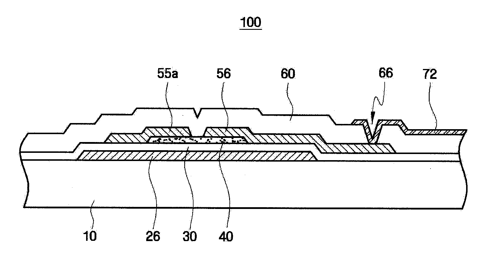
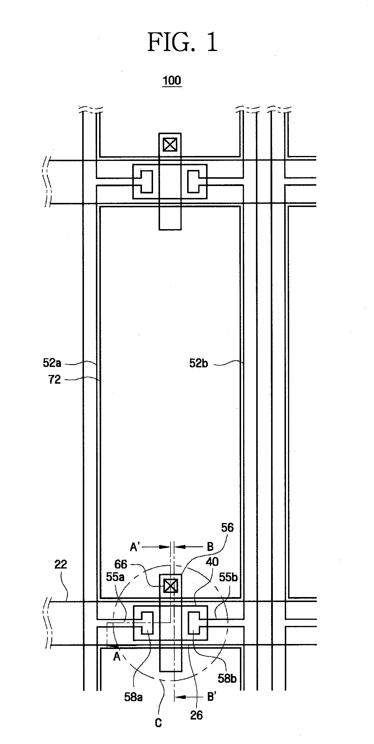
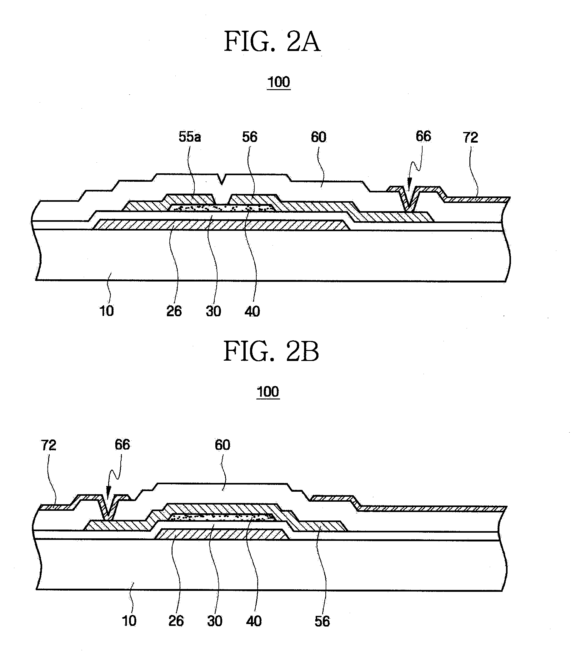
[0025]Advantages and features of the present disclosure and methods of accomplishing the same may be understood more readily by reference to the following detailed description of exemplary embodiments and the accompanying drawings. The exemplary embodiments provided herein are to be taken as nonlimiting. Like reference numerals refer to like elements throughout the specification.

[0026]It will be understood that when an element or layer is referred to as being “on”, “connected to” or “coupled to” another element or layer, it can be directly on, connected or coupled to the other element or layer or intervening elements or layers may be present. In contrast, when an element is referred to as being “directly on”, “directly connected to” or “directly coupled to” another element or layer, there are no intervening elements or layers present. Like numbers refer to like elements throughout the specification.

[0027]Spatially relative terms, such as “beneath”, “below”, “lower”, “above”, “upper”...


PUM


Abstract

A thin film transistors (TFTs) substrate is structured to maintain as constant across the area of the substrate a kickback voltage due to Miller capacitance between the drain and gate of each TFT even in the presence of manufacturing induced misalignments between the drain electrodes and corresponding gate lines. Each thin film transistor includes a gate electrode, an active layer formed on the gate electrode so as to overlap the gate electrode, first and second source electrodes respectively connected to first and second data lines each of which crosses the gate line while being insulated from the gate line, and an elongated drain electrode located between the first and second source electrodes and disposed over the gate electrode so as to a crossing length of the drain electrode is larger than an underlying width of the gate electrode such that misalignment induced shifts of the position of the gate electrode relative to the drain electrode does not substantially change overlap area between the two.

Description

CROSS REFERENCE TO RELATED APPLICATION[0001]This application claims priority from Korean Patent Application No. 10-2006-0097144 filed on Oct. 2, 2006 in the Korean Intellectual Property Office, the disclosure of which is incorporated herein by reference in its entirety.BACKGROUND[0002]1. Field of Invention[0003]The present disclosure of invention relates to a thin film transistor (TFT) substrate, and more particularly, to a thin film transistor substrate such as may be used in flat panel display applications and is capable of providing improved image quality in an image display device by maintaining a substantially constant drain-to-gate feedback capacitance even in the presence of mask misalignment.[0004]2. Description of Related Art[0005]Generally, flat panel image display devices include a thin film transistor (TFT) array formed on a transparent substrate that has interconnect electrodes provided thereon. Such flat panel devices display a predetermined but changeable (i.e., movin...

Claims


Application Information

Patent Timeline
IPC IPC(8): H01L51/10
CPCH01L27/283H01L27/3262H01L27/285H10K19/202H10K19/10H10K59/1213H10K10/84
Inventor YANG, SUNG-HOONKIM, SO-WOONHWANG, TAE-HYUNGKIM, YEON-JOOYOON, SOO-WANCHAI, CHONG-CHUL
Owner SAMSUNG DISPLAY CO LTD
Why Eureka
Try Eureka