Auto-nulled bandgap reference system and strobed bandgap reference circuit

Active Publication Date: 2008-04-03
ANALOG DEVICES INC
View PDF1 Cites 7 Cited by
  • Summary
  • Abstract
  • Description
  • Claims
  • Application Information

AI Technical Summary

Benefits of technology

[0006]It is a further object of this invention to provide such an improved auto-nulled bandgap reference system which removes or at least reduces both the offset and low frequency noise effects of the amplifier.
[0007]It is a further object of this invention to provide such an improved auto-nulled bandgap reference system which reduces the voltage shift of the reference over temperature.
[0008]It is a further object of this invention to provide such an improved auto-nulled bandgap reference system which re-locates or spreads the noise within the pass band of the intended application.
[0009]It is a further object of this invention to provide such an improved auto-nulled bandgap reference system which can apply the auto-nulling effect at a constant frequency, by frequency hopping or by random or spread spectrum frequency techniques.
[0012]It is a further object of this invention to provide such an improved strobed bandgap reference circuit which can reduce the average supply current by a factor or 1000 or more.
[0014]The invention further realizes that a significant reduction in average power required to operate auto-nulled and other bandgap references can be accomplished with a strobe circuit including an output storage device and a strobe control circuit for periodically powering up a bandgap reference circuit to charge the output storage device and powering down the bandgap reference circuit to conserve power.

Problems solved by technology

As the semiconductor industry continues to mature, cost pressures persist that drive companies to continually reduce manufacturing costs.
A consequence of the reduced process feature set is the removal of dedicated (non-substrate) bipolar devices that would require extra processing steps, and therefore cost, to implement.
However since dedicated bipolar devices are not available in most reduced feature set processes of today, MOS devices must typically be used.
The larger and less predictable device mismatch levels in MOS devices result in larger and less predictable circuit performances both for initial tolerances and drift over temperature.
Additionally, increasing relative noise levels in circuits using MOS devices are exacerbated by reductions in process line width due to thinner gate oxides.
The increased noise levels and larger voltage shifts over temperature resulting from MOS devices are un-desirable features in a voltage reference.
This leaves the non-idealities of the MOS amplifier, input referred offset, temperature drift, and noise, as the dominant error sources in the reference.
Though this gain can be minimized by increasing the PTAT voltage, practical limitations on the ratio of current densities in the substrate bipolar junction transistors place the gain factor (on a single bandgap) in the 8×-12× range.
Thus, random drift offsets, and low frequency noise of the MOS amplifier are the main impediment for achieving a tight temperature coefficient specification for the reference.

Method used


Image

  • Auto-nulled bandgap reference system and strobed bandgap reference circuit
  • Auto-nulled bandgap reference system and strobed bandgap reference circuit
  • Auto-nulled bandgap reference system and strobed bandgap reference circuit

Examples


Embodiment Construction

[0031]Aside from the preferred embodiment or embodiments disclosed below, this invention is capable of other embodiments and of being practiced or being carried out in various ways. Thus, it is to be understood that the invention is not limited in its application to the details of construction and the arrangements of components set forth in the following description or illustrated in the drawings. If only one embodiment is described herein, the claims hereof are not to be limited to that embodiment. Moreover, the claims hereof are not to be read restrictively unless there is clear and convincing evidence manifesting a certain exclusion, restriction, or disclaimer.

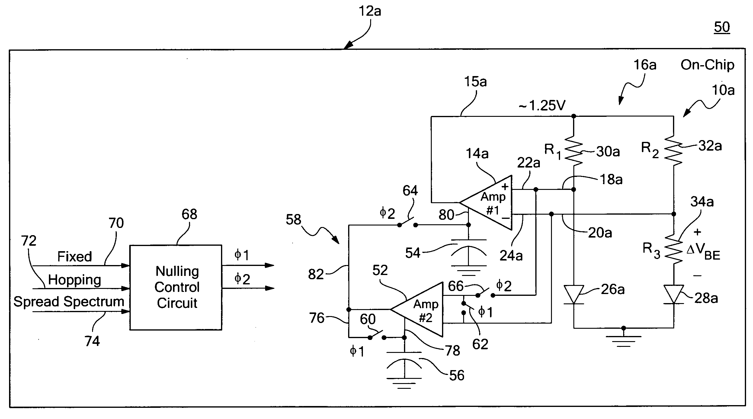
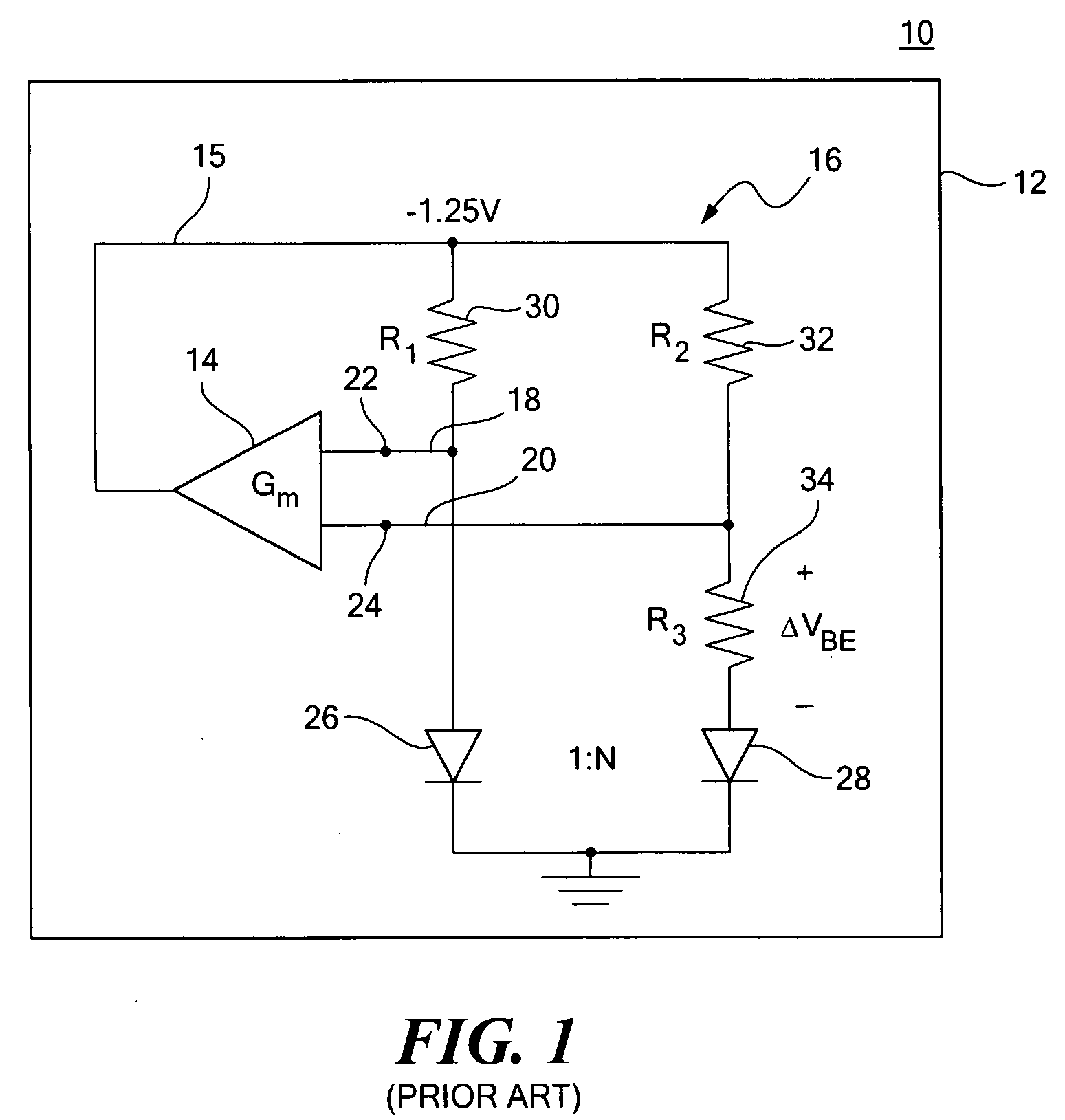
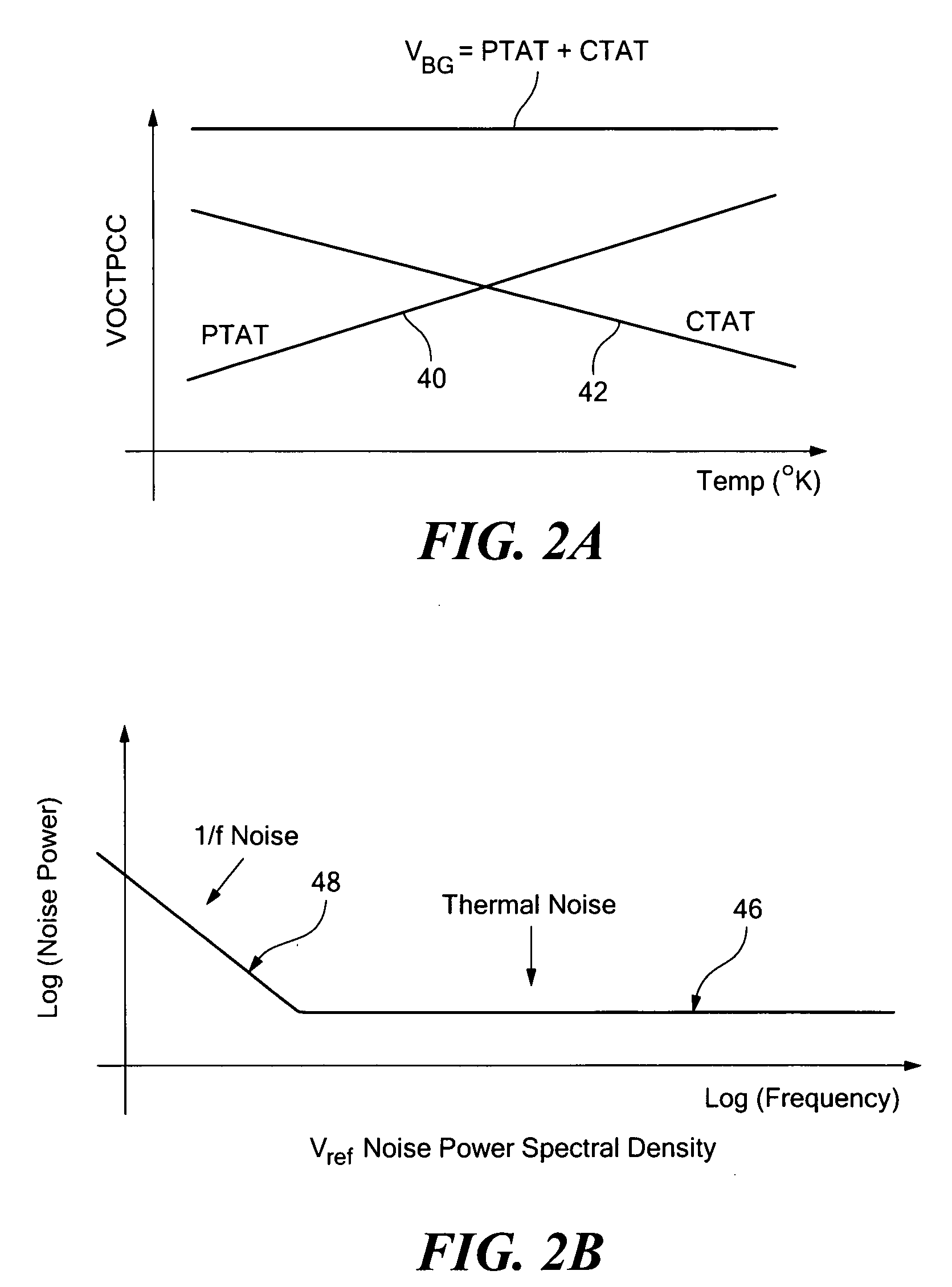
[0032]There is shown in FIG. 1 a basic substrate bandgap reference circuit 10 contained on the single MOS chip 12 including an amplifier 14 and a substrate PTAT bandgap core 16 which has a differential output 18, 20 to the differential input 22, 24 of amplifier 14. Amplifier 14 operates with a feedback circuit 15 which resp...


PUM


Abstract

An auto-nulled bandgap reference system employing a substrate bandgap reference circuit with primary and auxiliary amplifiers and a switching circuit which in a first mode develops a voltage to null the offset and noise errors of the auxiliary amplifier and then in the second mode uses the nulled auxiliary amplifier to develop a voltage to null the offset and noise errors of the primary amplifier; and a strobe circuit including an output storage device and a strobe control circuit for periodically powering up a bandgap reference circuit to charge the output storage device and powering down the bandgap reference circuit to conserve power.

Description

RELATED APPLICATIONS[0001]This application claims benefit of and priority to U.S. Provisional Application Ser. No. 60 / 848,919 filed Oct. 3, 2006 incorporated herein by this reference.FIELD OF THE INVENTION[0002]This invention relates to an auto-nulled bandgap reference system and also to a strobed bandgap reference circuit adapted for use with an auto-nulled or other bandgap reference.BACKGROUND OF THE INVENTION[0003]As the semiconductor industry continues to mature, cost pressures persist that drive companies to continually reduce manufacturing costs. A direct result of this pricing pressure is the movement to smaller geometry fabrication processes with reduced feature sets. A consequence of the reduced process feature set is the removal of dedicated (non-substrate) bipolar devices that would require extra processing steps, and therefore cost, to implement. Note bipolar devices typically exhibit substantially smaller (and more predictable over temperature) offset voltages and have ...

Claims


Application Information

Patent Timeline
IPC IPC(8): G05F3/16
CPCG05F3/30
Inventor ASHBURN, MICHAEL A.HARSTON, STEPHEN W.
Owner ANALOG DEVICES INC
Why Eureka
Try Eureka