Edge connect wafer level stacking

a technology of edge connect and stacking, which is applied in the direction of electrical equipment, semiconductor devices, semiconductor/solid-state device details, etc., can solve the problems of substrate cracking during the notching process, and achieve the effects of reducing cost, reducing weight, and reducing siz

Active Publication Date: 2008-04-10
TESSERA INC
View PDF98 Cites 148 Cited by
  • Summary
  • Abstract
  • Description
  • Claims
  • Application Information

AI Technical Summary

Benefits of technology

[0009] The present invention provides apparatus and methods for production of integrated circuit devices to create stacked microelectronic packages suitable for processing at a wafer level to produce integrated circuits of lower cost, smaller size, lower weight, enhanced electrical performance.

Problems solved by technology

It has been found that without such cavities, there is a propensity for the substrate to crack during the notching process.

Method used


Image

  • Edge connect wafer level stacking
  • Edge connect wafer level stacking
  • Edge connect wafer level stacking

Examples


Embodiment Construction

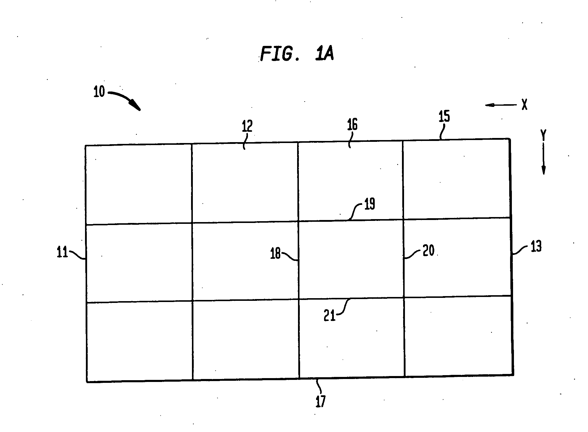
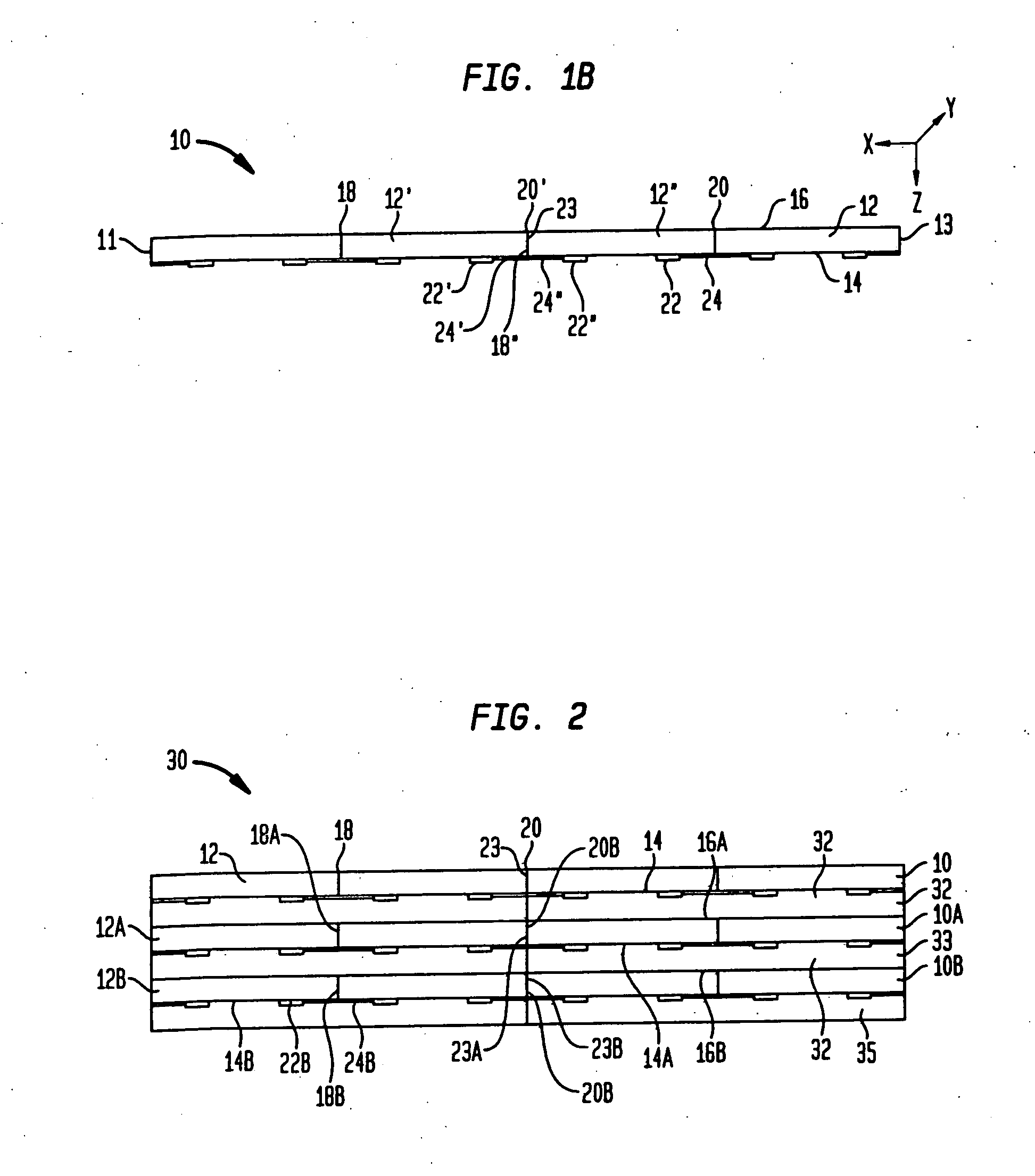
[0049] Reference is now made to FIGS. 1-4B, which illustrate a method and apparatus for stacking microelectronic components. As shown in FIGS. 1A-1B, a portion of a first wafer or subassembly 10 includes a plurality of microelectronic elements 12, each positioned side by side and adjacent to one another. The first wafer or subassembly 10 preferably includes numerous rows of microelectronic elements 12 aligned along an X-axis and a Y-axis. The microelectronic elements are formed integral with one another using conventional semiconductor process techniques. It should be apparent that the subassembly 10 may be a portion of a wafer. The subassembly may have additional elements attached thereto (not shown). The subassembly may be in the shape of a circular wafer.

[0050] Each microelectronic element 12 includes a front face 14 (FIG. 1B) and an oppositely-facing rear face 16. The microelectronic elements 12 also include first edges 18, second edges 20, third edges 19 and fourth edges 21, a...


PUM


Abstract

A method of making a stacked microelectronic package by forming a microelectronic assembly by stacking a first subassembly including a plurality of microelectronic elements onto a second subassembly including a plurality of microelectronic elements, at least some of the plurality of microelectronic elements of said first subassembly and said second subassembly having traces that extend to respective edges of the microelectronic elements, then forming notches in the microelectronic assembly so as to expose the traces of at least some of the plurality of microelectronic elements, then forming leads at the side walls of the notches, the leads being in electrical communication with at least some of the traces and dicing the assembly into packages. Additional embodiments include methods for creating stacked packages using substrates and having additional traces that extend to both the top and bottom of the package.

Description

REFERENCE TO RELATED APPLICATIONS [0001] This application claims the benefit of the filing date of U.S. Provisional Patent Application No. 60 / 850,850 filed Oct. 10, 2006, the disclosure of which is hereby incorporated herein by reference.BACKGROUND OF THE INVENTION [0002] The present invention generally relates to stacked microelectronic packages and more particularly relates to stacked microelectronic packages fabricated at the wafer level and to methods of making such packages. [0003] Semiconductor chips are flat bodies with contacts disposed on the front surface that are connected to the internal electrical circuitry of the chip itself. Semiconductor chips are typically packaged with substrates to form microelectronic packages having terminals that are electrically connected to the chip contacts. The package may then be connected to test equipment to determine whether the packaged device conforms to a desired performance standard. Once tested, the package may be connected to a la...

Claims


Application Information

Patent Timeline
Patent Type & Authority Applications(United States)
IPC IPC(8): H01L23/48H01L21/58
CPCH01L23/481H01L21/30604H01L24/82H01L24/94H01L25/0657H01L25/50H01L2224/16H01L2224/24145H01L2224/83855H01L2225/06551H01L2225/06555H01L2225/06586H01L2225/06596H01L2924/01029H01L2924/01078H01L2924/01082H01L2924/14H01L2224/9202H01L2924/01005H01L2924/01006H01L2924/01033H01L2924/014H01L24/83H01L24/24H01L2924/3512H01L2924/00H01L2224/92244H01L2224/05548H01L2224/05573H01L2924/00014H01L2224/0554H01L2224/02377H01L2224/05599H01L2224/0555H01L2224/0556H01L21/78
Inventor HABA, BELGACEMOGANESIAN, VAGE
Owner TESSERA INC
Why Eureka
Try Eureka