Data receiver and semiconductor device including the data receiver

a data receiver and semiconductor technology, applied in the field of data receivers, can solve the problems of increasing data transmission speed, increasing isi, and limited maximum operation speed of a semiconductor device (for example a dram), so as to reduce circuit size and power consumption, and avoid timing delays

Active Publication Date: 2008-04-17
SAMSUNG ELECTRONICS CO LTD
View PDF5 Cites 19 Cited by
  • Summary
  • Abstract
  • Description
  • Claims
  • Application Information

AI Technical Summary

Benefits of technology

[0021]To solve the above and/or other problems, the embodiments of the present invention provide a loop unrolling DFE receiver that uses analog control signals from each equalizer to avoid timing delays associated with the use of latched digital control signals in the conventio

Problems solved by technology

However, in the improvement of system performance, the increase of the data transmission speed is restricted due to the physical limit of a channel.
In particular, the ISI becomes more severe on a dynamic random access memory (DRAM).
However, in the single tap DFE receiver 10, the feedback loop that i

Method used


Image

  • Data receiver and semiconductor device including the data receiver
  • Data receiver and semiconductor device including the data receiver
  • Data receiver and semiconductor device including the data receiver

Examples


Embodiment Construction

[0033]The attached drawings for illustrating embodiments of the present invention are referred to in order to gain a sufficient understanding of the present invention, the merits thereof, and the objectives accomplished by the implementation of the present invention.

[0034]Hereinafter, the present invention will be described in detail by explaining embodiments of the invention with reference to the attached drawings. Like reference numerals in the drawings denote like elements.

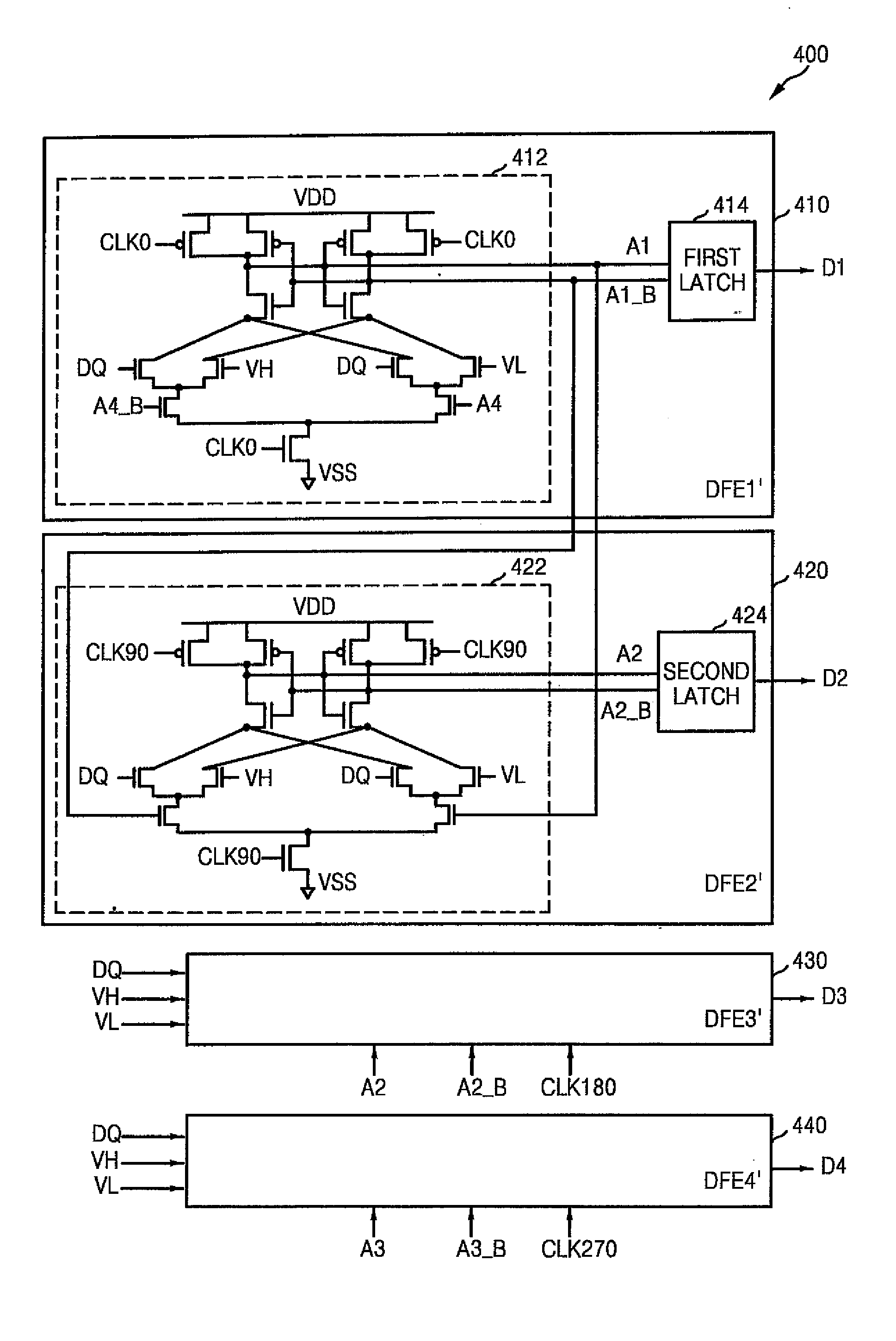
[0035]FIG. 4 is a circuit diagram of a four interleaved loop unrolling DFE receiver 400 according to an embodiment of the present invention. FIG. 5 is a circuit diagram of third and fourth equalizers of FIG. 4. Referring to FIGS. 4 and 5, the receiver 400 includes a first equalizer DFE1′410, a second equalizer DFE2′420, a third equalizer DFE3′430, and a fourth equalizer DFE4′440. Each of the equalizers 410 through 440 has the same structure except for input and output signals.

[0036]Each of the first through fou...


PUM


Abstract

The invention is directed to data receivers such as those used in semiconductor devices. Embodiments of the invention provide a loop unrolling DFE receiver that uses analog control signals from each equalizer to avoid timing delays associated with the use of latched digital control signals in the conventional art. In addition, embodiments of the invention implement each equalizer with a single sense amplifier based flip flop (SAFF) to reduce circuit size and power consumption

Description

BACKGROUND OF THE INVENTION[0001]1. Field of the Invention[0002]The present invention relates generally to a data receiver, and more particularly, but not by way of limitation, to a data receiver of a semiconductor device.[0003]This application claims the benefit of Korean Patent Application No. 10-2006-0100513, filed on Oct. 16, 2006, in the Korean Intellectual Property Office, the disclosure of which is incorporated herein in its entirety by reference.[0004]2. Description of the Related Art[0005]The data transmission speed between semiconductor chips has increased. However, in the improvement of system performance, the increase of the data transmission speed is restricted due to the physical limit of a channel. A transmission line on a printed circuit board (PCB) has a feature of a low pass filter. Accordingly, when a data signal is transmitted at a speed of several gigabits per second (Gb / s), a gain of the transmitted data signal through the transmission line decreases, and inter...

Claims


Application Information

Patent Timeline
IPC IPC(8): G11C7/06
CPCG11C7/1078G11C11/4093G11C7/1087H04L27/01
Inventor BAE, SEUNG-JUN
Owner SAMSUNG ELECTRONICS CO LTD
Why Eureka
Try Eureka