
Size-reduced layout of cell-based integrated circuit with power switch

a cell-based integrated circuit and power switch technology, applied in the field of semiconductor integrated circuits, can solve the problems of increasing circuit size, total power consumption, increasing leak current, etc., and achieve the effect of reducing the circuit size of cell-based integrated circuits

Inactive Publication Date: 2008-04-24
NEC ELECTRONICS CORP
View PDF7 Cites 22 Cited by
  • Summary
  • Abstract
  • Description
  • Claims
  • Application Information

AI Technical Summary

Benefits of technology

"The present invention provides an integrated circuit with a smaller size for controlling power supply to cells in the non-operating state. This is achieved by providing a well along the first power line and a plurality of power switch transistors connected to the first power line and the additional power lines. A bias voltage is fed to the well through both of the first and second well contacts, which are connected to the first and second additional power lines, respectively. This reduces the circuit size of cell-based integrated circuits and improves their efficiency."

Problems solved by technology

The increase in the leak current is one of the major issues in device dimension reduction of semiconductor integrated circuits.
When a cell-based integrated circuit is placed into standby mode, the power consumption is desirably reduced as low as possible; however leak currents through deactivated primitive cells often account for a major part of the total power consumption.
One drawback of the conventional integrated circuit shown in FIG. 11 is the increased circuit size.

Method used


Image

  • Size-reduced layout of cell-based integrated circuit with power switch
  • Size-reduced layout of cell-based integrated circuit with power switch
  • Size-reduced layout of cell-based integrated circuit with power switch

Examples


first embodiment

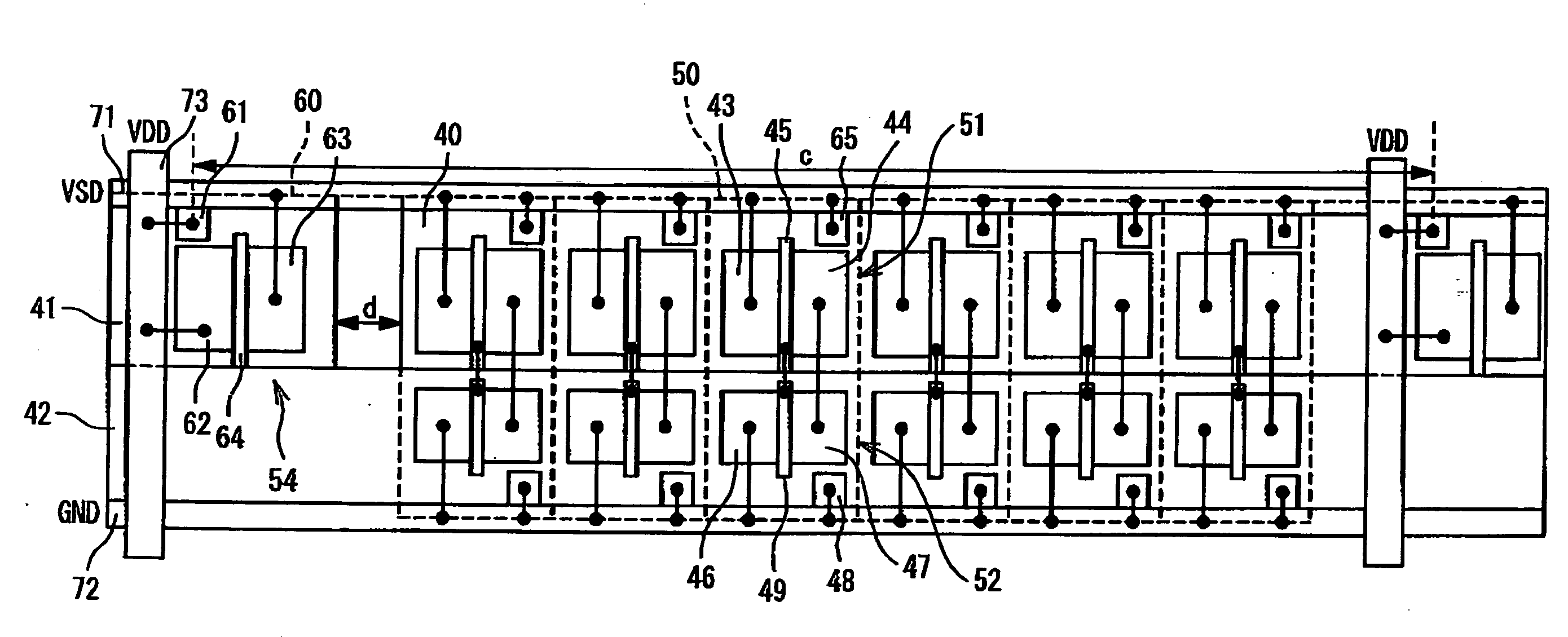
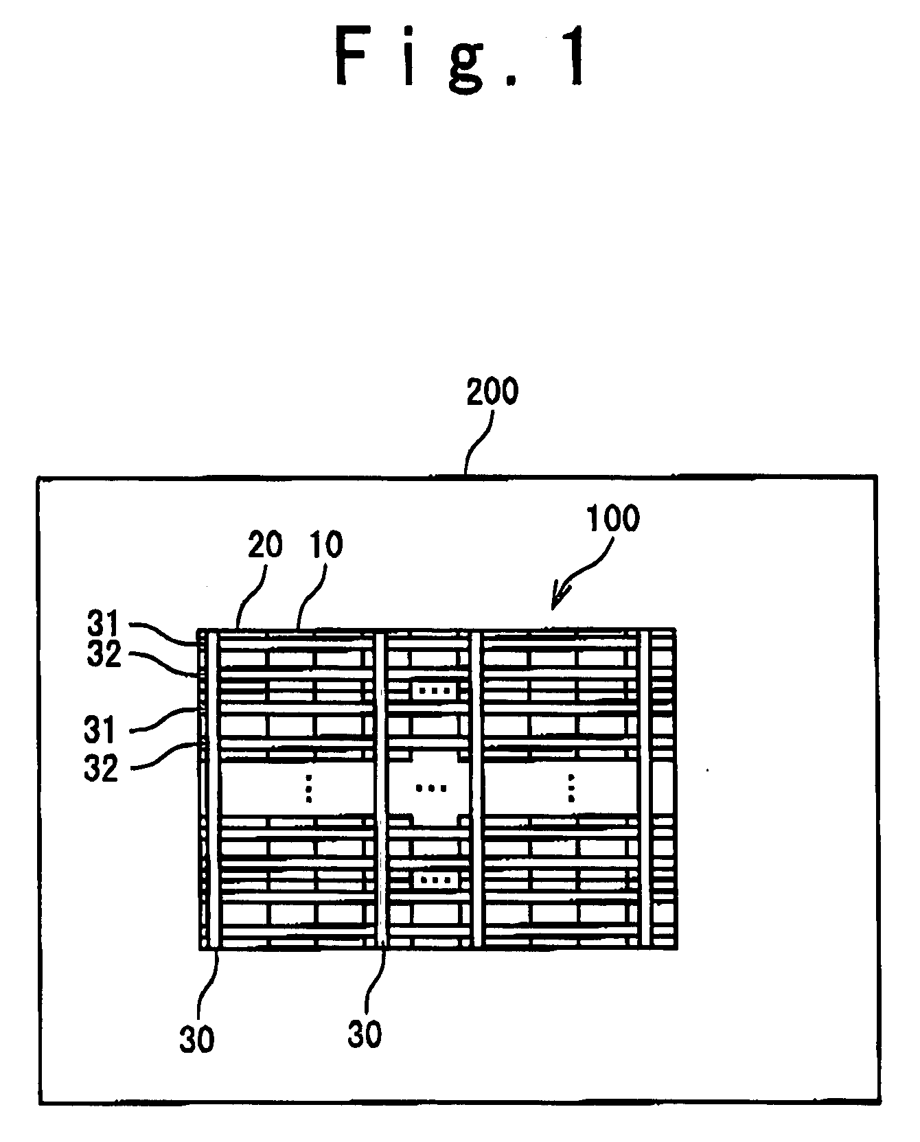
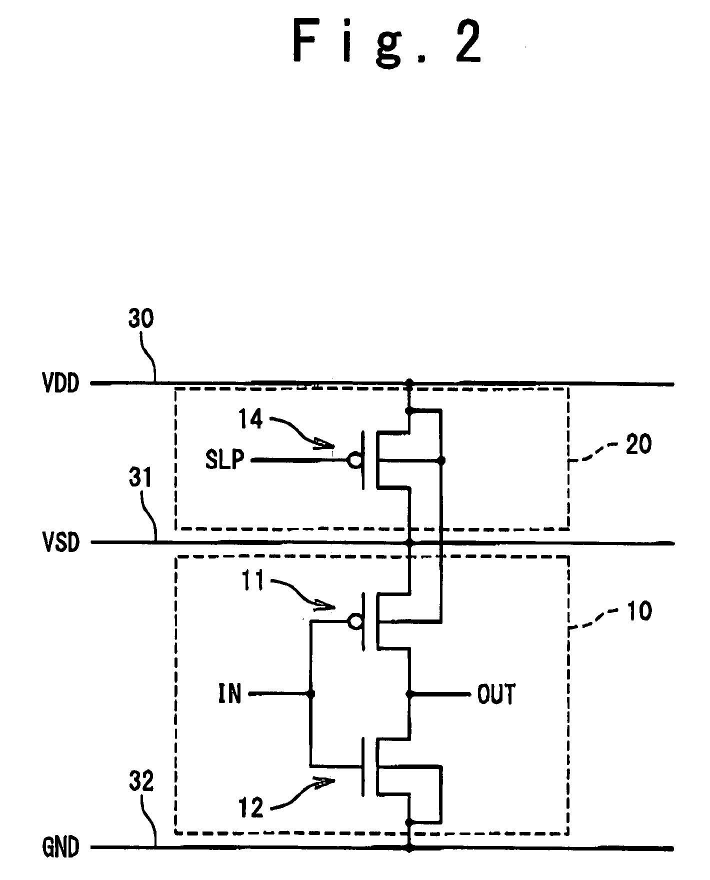
[0031]Referring to FIG. 1 to 6, an integrated circuit 200 of a first embodiment of the present embodiment will be described in the following. FIG. 1 is a plain view of the integrated circuit 200 in the first embodiment. The integrated circuit 200 includes a functional cell 100. The functional cell 100 includes primitive cells 10, power switch cells 20, VDD power lines 30, VSD power lines 31, and ground lines 32. VDD power lines 30 intersect with the VSD power lines 31 and the ground lines 32. The primitive cells 10 are arranged in rows and columns in the functional cell 100. The primitive cells 10 each include a logic circuit designed with CMOS architecture. The power switch cells 20 control the power supply to the primitive cells 10 within the function cell 100. The logic circuits within the primitive cells 10 operate on the power source voltage and the ground voltage supplied from the VSD power lines 31 and the ground lines 32, respectively. The power switch cells 20 supply the po...

second embodiment

[0049]A description is given of an integrated circuit 200 of a second embodiment of the present invention, referring to FIG. 7 to 10. In the second embodiment, different power source voltages are supplied as the substrate and source biases of the power switch cells 20; it should be noted that, in the first embodiment, the power source voltage VDD is commonly supplied as the substrate and source biases.

[0050]FIG. 7 is a plain view of the integrated circuit 200 of the second embodiment. In this embodiment, the functional cell 100 is provided with VDD1 power lines 33 and VDD2 power lines 34, instead of the VDD power lines 31. The VDD1 power lines 33 and VDD2 power lines 34 are fed with separately-generated power source voltages; the VDD1 power lines 33 are fed with a power source voltage VDD1 while the VDD2 power lines 34 are fed with a power source voltage VDD2. Other configurations of the functional cell 100 of the second embodiment are the same as those of the functional cell 100 of...


PUM


Abstract

An integrated circuit is provided with a first power line, a plurality of additional power lines intersecting with the first power line, a plurality of power switch transistors each having a drain connected with the first power line and a source connected with one of the additional power lines, a well provided to extend along the first power line; and a plurality of primitive cells each including a first transistor prepared within the well, the first transistor having a source connected with the first power line. The plurality of additional power lines includes first and second additional power lines The plurality of primitive cells are provided between the first and second additional power lines along the first power line. A bias voltage is fed to the well through both of first and second well contacts, the first well contact providing a connection between the first additional power line and the well, and the second well contact providing a connection between the second additional power line and the well.

Description

[0001]This application claims the benefit of priority based on Japanese Patent Application No. 2006-285404, filed on Oct. 19, 2006, the disclosure of which is incorporated herein by reference.BACKGROUND OF THE INVENTION[0002]1. Field of the invention[0003]The present invention relates to a semiconductor integrated circuit, more particularly, to a cell-based integrated circuit with power switches that control the power supply to primitive cells.[0004]2. Description of the Related Art[0005]The increase in the leak current is one of the major issues in device dimension reduction of semiconductor integrated circuits. This also applies to cell-based integrated circuits. When a cell-based integrated circuit is placed into standby mode, the power consumption is desirably reduced as low as possible; however leak currents through deactivated primitive cells often account for a major part of the total power consumption. One approach for addressing this problem is to stop the power supply to t...

Claims


Application Information

Patent Timeline
Patent Type & Authority Applications(United States)
IPC IPC(8): H01L23/528
CPCH01L23/5286H01L27/0207H01L27/11807H01L2924/0002H01L2924/00
Inventor SAKURABAYASHI, TARO
Owner NEC ELECTRONICS CORP
Learn More