
Adaptive integrated circuitry with heterogeneous and reconfigurable matrices of diverse and adaptive computational units having fixed, application specific computational elements

a technology of adaptive integrated circuits and computational units, applied in general purpose stored program computers, instruments, sustainable buildings, etc., can solve the problems of reducing the efficiency consuming significantly more power, and comparatively inefficient processing of actual algorithmic operations, so as to reduce potential disadvantages, maximize the various advantages of processors, and reduce the effect of potential disadvantages

Inactive Publication Date: 2008-04-24
ALTERA CORP +1
View PDF12 Cites 5 Cited by
  • Summary
  • Abstract
  • Description
  • Claims
  • Application Information

AI Technical Summary

Benefits of technology

[0010] The present invention provides a new form or type of integrated circuitry which effectively and efficiently combines and maximizes the various advantages of processors, ASICs and FPGAs, while minimizing potential disadvantages. In accordance with the present invention, such a new form or type of integrated circuit, referred to as an adaptive computing engine (“ACE”), is disclosed which provides the programming flexibility of a processor, the post-fabrication flexibility of FPGAs, and the high speed and high utilization factors of an ASIC. The ACE integrated circuitry of the present invention is readily reconfigurable, in real time, and is capable of having corresponding, multiple modes of operation. In selected embodiments, the ACE may also minimize power consumption while increasing performance, with particular suitability for low power applications, such as for use in hand-held and other battery-powered devices.

Problems solved by technology

In addition, as processors are designed for the execution of instructions, large areas of the IC are allocated to instruction processing, with the result that the processors are comparatively inefficient in the performance of actual algorithmic operations, with only a few percent of these operations performed during any given clock cycle.
Microprocessors and DSPs, moreover, have a comparatively limited activity factor, such as having only approximately five percent of their transistors engaged in algorithmic operations at any given time, with most of the transistors allocated to instruction processing.
As a consequence, for the performance of any given algorithmic operation, processors consume significantly more IC (or silicon) area and consume significantly more power compared to other types of ICs, such as ASICs.
Once etched, however, an ASIC is not readily changeable, with any modification being time-consuming and expensive, effectively requiring new masks and new fabrication.
As a further result, ASIC design virtually always has a degree of obsolescence, with a design cycle lagging behind the evolving standards for product implementations.
The reconfiguring process for an FPGA is comparatively slow, however, and is typically unsuitable for most real time, immediate applications.
While this post-fabrication flexibility of FPGAs provides a significant advantage, FPGAs have corresponding and inherent disadvantages.
Compared to ASICs, FPGAs are very expensive and very inefficient for implementation of particular functions, and are often subject to a “combinatorial explosion” problem.
More particularly, for FPGA implementation, an algorithmic operation comparatively may require orders of magnitude more IC area, time and power, particularly when the particular algorithmic operation is a poor fit to the pre-existing, homogeneous islands of logic gates of the FPGA material.
In addition, the programmable interconnect, which should be sufficiently rich and available to provide reconfiguration flexibility, has a correspondingly high capacitance, resulting in comparatively slow operation and high power consumption.
For example, compared to an ASIC, an FPGA implementation of a relatively simple function, such as a multiplier, consumes significant IC area and vast amounts of power, while providing significantly poorer performance by several orders of magnitude.
In addition, there is a chaotic element to FPGA routing, rendering FPGAs subject to unpredictable routing delays and wasted logic resources, typically with approximately one-half or more of the theoretically available gates remaining unusable due to limitations in routing resources and routing algorithms.
Various prior art attempts to meld or combine these various processor, ASIC and FPGA architectures have had utility for certain limited applications, but have not proven to be successful or useful for low power, high efficiency, and real time applications.
Typically, these prior art attempts have simply provided, on a single chip, an area of known FPGA material (consisting of a repeating array of identical logic gates with interconnect) adjacent to either a processor or an ASIC, with limited interoperability, as an aid to either processor or ASIC functionality.
This reprogrammable instruction set accelerator, while allowing for some post-fabrication reconfiguration flexibility and processor acceleration, is nonetheless subject to the various disadvantages of traditional processors and traditional FPGA material, such as high power consumption and high capacitance, with comparatively low speed, low efficiency and low activity factors.
While potentially providing post-fabrication means for “bug fixes” and other error correction, the prior art IC is nonetheless subject to the various disadvantages of traditional ASICs and traditional FPGA material, such as highly limited reprogrammability of an ASIC, combined with high power consumption, comparatively low speed, low efficiency and low activity factors of FPGAs.

Method used


Image

  • Adaptive integrated circuitry with heterogeneous and reconfigurable matrices of diverse and adaptive computational units having fixed, application specific computational elements
  • Adaptive integrated circuitry with heterogeneous and reconfigurable matrices of diverse and adaptive computational units having fixed, application specific computational elements
  • Adaptive integrated circuitry with heterogeneous and reconfigurable matrices of diverse and adaptive computational units having fixed, application specific computational elements

Examples


Embodiment Construction

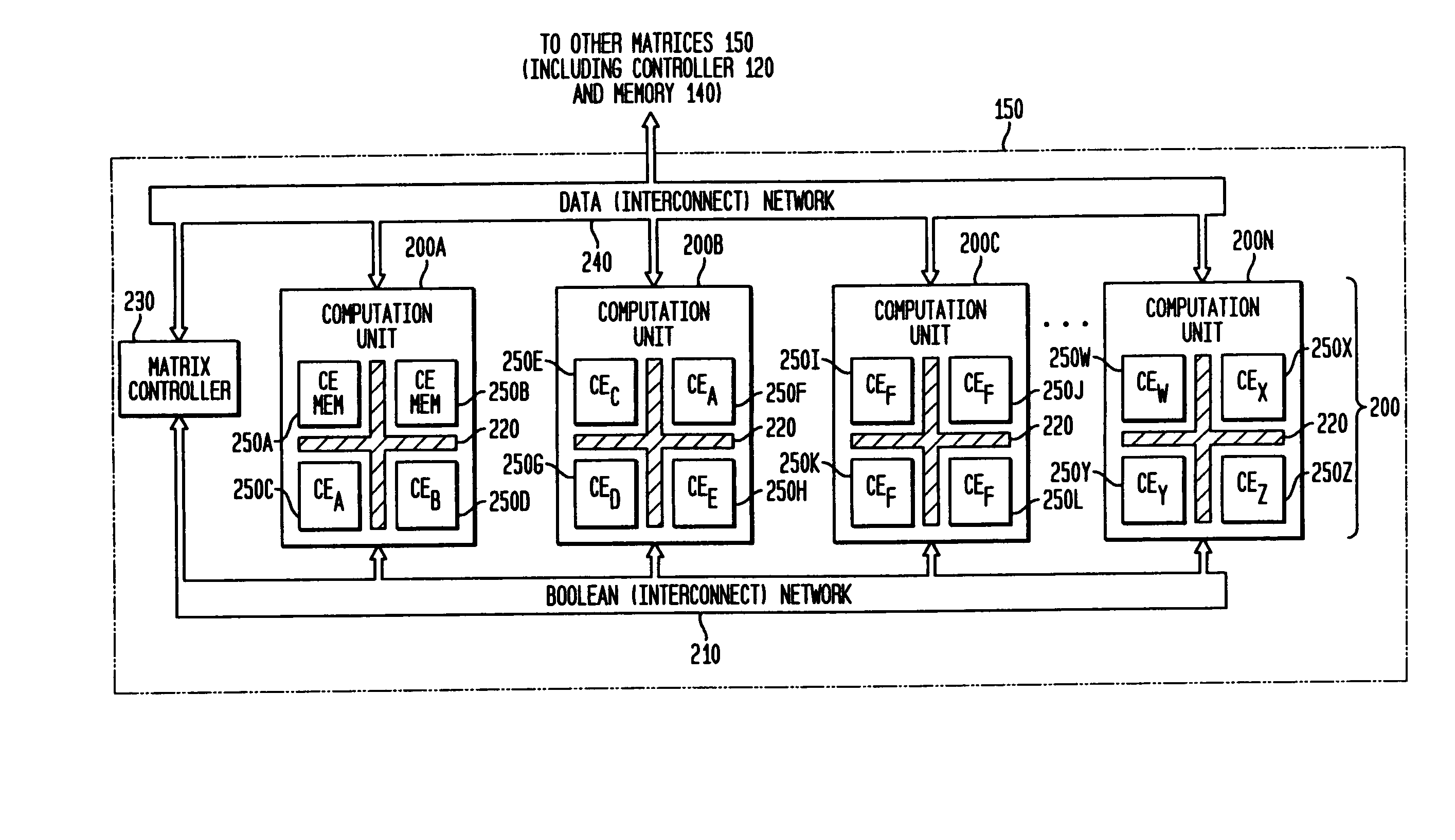
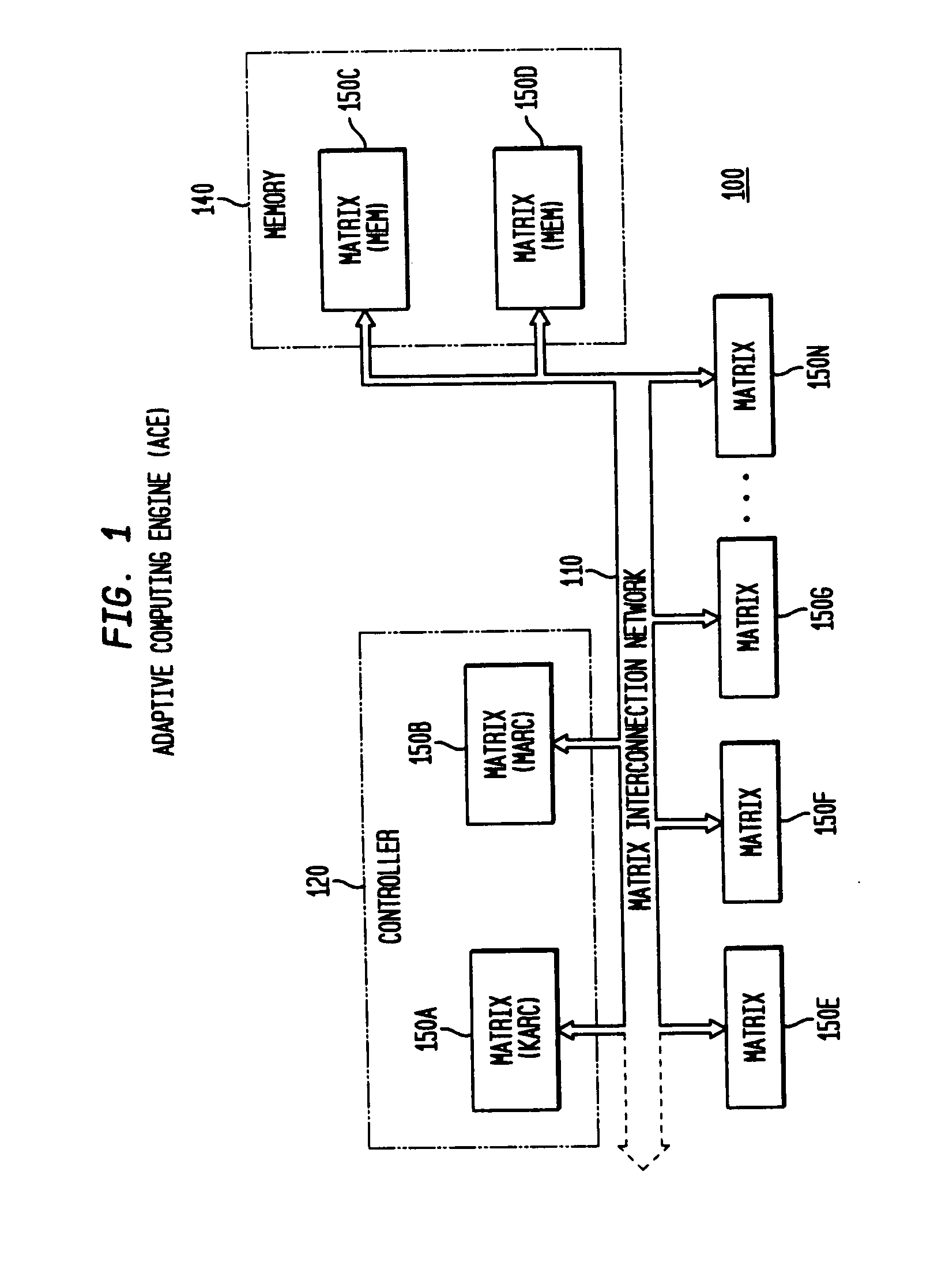
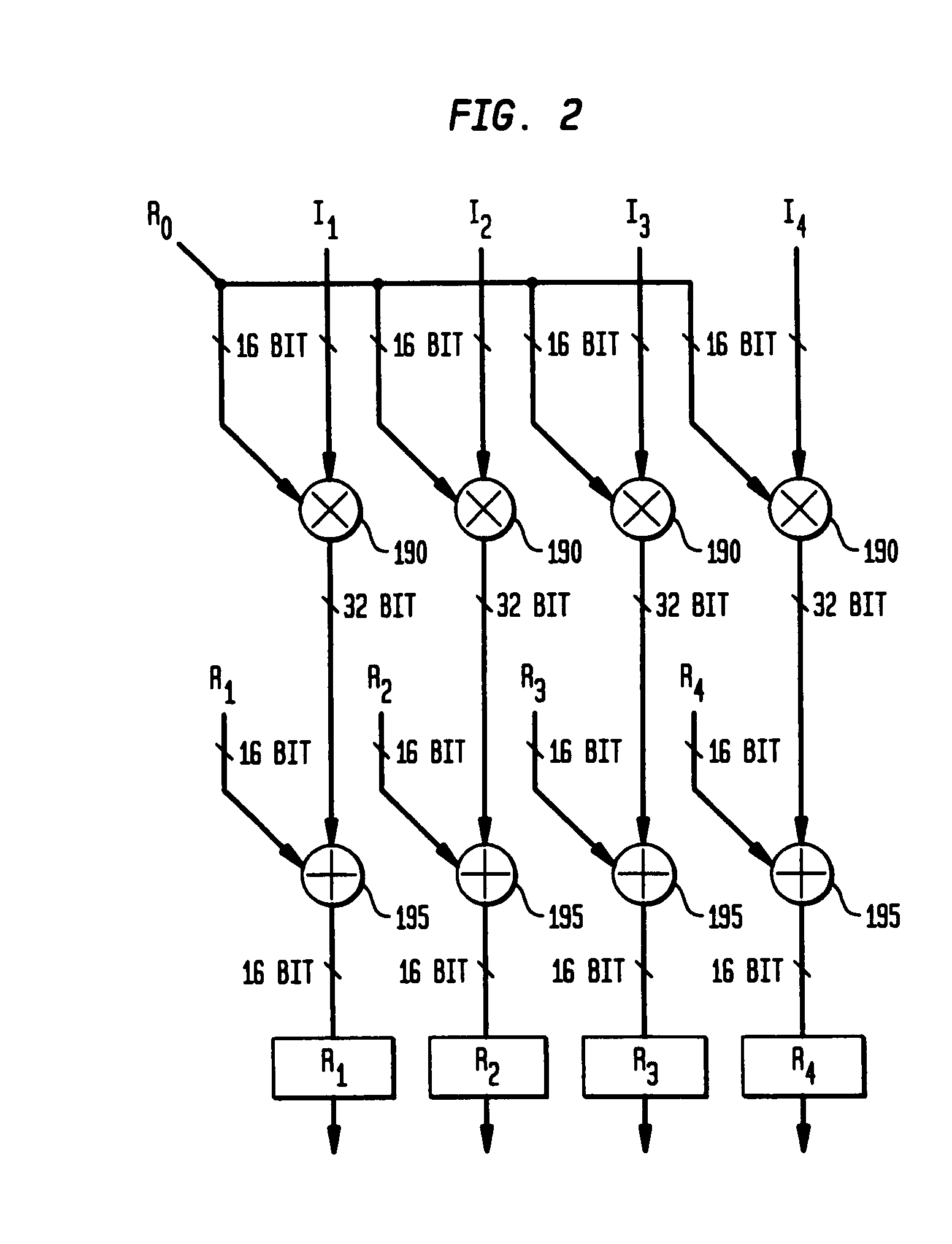
[0029] While the present invention is susceptible of embodiment in many different forms, there are shown in the drawings and will be described herein in detail specific embodiments thereof, with the understanding that the present disclosure is to be considered as an exemplification of the principles of the invention and is not intended to limit the invention to the specific embodiments illustrated.

[0030] As indicated above, the present invention provides a new form or type of integrated circuit, referred to as an adaptive computing engine (ACE), which provides the programming flexibility of a processor, the post-fabrication flexibility of FPGAs, and the high speed and high utilization factors of an ASIC. The ACE integrated circuitry of the present invention is readily adaptive (or reconfigurable), in real time, and is capable of having corresponding, multiple modes of operation. The present invention may also be utilized to minimize power consumption while increasing performance, w...


PUM


Abstract

The present invention provides an adaptive integrated circuit. The various embodiments include a plurality of heterogeneous computational elements coupled to an interconnection network. The plurality of heterogeneous computational elements include corresponding computational elements having fixed and differing architectures, such as fixed architectures for different functions such as memory, addition, multiplication, complex multiplication, subtraction, configuration, reconfiguration, control, input, output, and field programmability. In response to configuration information, the interconnection network is operative in real time to configure and reconfigure the plurality of heterogeneous computational elements for a plurality of different functional modes, including linear algorithmic operations, non-linear algorithmic operations, finite state machine operations, memory operations, and bit-level manipulations.

Description

CROSS-REFERENCE TO A RELATED APPLICATION [0001] This application is a continuation-in-part of Paul L. Master et al., U.S. patent application Ser. No. 09 / 815,122, entitled “Adaptive Integrated Circuitry With Heterogeneous And Reconfigurable Matrices Of Diverse And Adaptive Computational Units Having Fixed, Application Specific Computational Elements”, filed Mar. 22, 2001, commonly assigned to QuickSilver Technology, Inc., and incorporated by reference herein, with priority claimed for all commonly disclosed subject matter (the “related application”).FIELD OF THE INVENTION [0002] The present invention relates, in general, to integrated circuits and, more particularly, to adaptive integrated circuitry with heterogeneous and reconfigurable matrices of diverse and adaptive computational units having fixed, application specific computational elements. BACKGROUND OF THE INVENTION [0003] The advances made in the design and development of integrated circuits (“ICs”) have generally produced I...

Claims


Application Information

Patent Timeline
Patent Type & Authority Applications(United States)
IPC IPC(8): G06F15/177G06F15/78
CPCG06F15/7867Y02B60/1225Y02B60/1207Y02D10/00
Inventor MASTER, PAUL L.HOGENAUER, EUGENESCHEUERMANN, WALTER JAMES
Owner ALTERA CORP
Learn More