
Method and system for managing hardware resources to implement system functions using an adaptive computing architecture

a technology of adaptive computing and hardware resources, applied in the field of integrated circuits, can solve the problems of consuming significantly more power, reducing the efficiency and comparatively inefficient performance of actual algorithmic operations of processors, so as to achieve efficient and efficient combining and maximizing the various advantages of processors , the effect of minimizing potential disadvantages

Inactive Publication Date: 2010-07-06
ALTERA CORP
View PDF567 Cites 16 Cited by
  • Summary
  • Abstract
  • Description
  • Claims
  • Application Information

AI Technical Summary

Benefits of technology

[0014]The present invention provides a new form or type of integrated circuitry which effectively and efficiently combines and maximizes the various advantages of processors, ASICs and FPGAs, while minimizing potential disadvantages. In accordance with the present invention, such a new form or type of integrated circuit, referred to as an adaptive computing engine (ACE), is disclosed which provides the programming flexibility of a processor, the post-fabrication flexibility of FPGAs, and the high speed and high utilization factors of an ASIC. The ACE integrated circuitry of the present invention is readily reconfigurable, in real-time, is capable of having corresponding, multiple modes of operation, and further minimizes power consumption while increasing performance, with particular suitability for low power applications, such as for use in hand-held and other battery-powered devices.

Problems solved by technology

In addition, as processors are designed for the execution of instructions, large areas of the IC are allocated to instruction processing, with the result that the processors are comparatively inefficient in the performance of actual algorithmic operations, with only a few percent of these operations performed during any given clock cycle.
Microprocessors and DSPs, moreover, have a comparatively limited activity factor, such as having only approximately five percent of their transistors engaged in algorithmic operations at any given time, with most of the transistors allocated to instruction processing.
As a consequence, for the performance of any given algorithmic operation, processors consume significantly more IC (or silicon) area and consume significantly more power compared to other types of ICs, such as ASICs.
Once etched, however, an ASIC is not readily changeable, with any modification being time-consuming and expensive, effectively requiring new masks and new fabrication.
As a further result, ASIC design virtually always has a degree of obsolescence, with a design cycle lagging behind the evolving standards for product implementations.
The reconfiguring process for an FPGA is comparatively slow, however, and is typically unsuitable for most real-time, immediate applications.
While this post-fabrication flexibility of FPGAs provides a significant advantage, FPGAs have corresponding and inherent disadvantages.
Compared to ASICs, FPGAs are very expensive and very inefficient for implementation of particular functions, and are often subject to a “combinatorial explosion” problem.
More particularly, for FPGA implementation, an algorithmic operation comparatively may require orders of magnitude more IC area, time and power, particularly when the particular algorithmic operation is a poor fit to the pre-existing, homogeneous islands of logic gates of the FPGA material.
In addition, the programmable interconnect, which should be sufficiently rich and available to provide reconfiguration flexibility, has a correspondingly high capacitance, resulting in comparatively slow operation and high power consumption.
For example, compared to an ASIC, an FPGA implementation of a relatively simple function, such as a multiplier, consumes significant IC area and vast amounts of power, while providing significantly poorer performance by several orders of magnitude.
In addition, there is a chaotic element to FPGA routing, rendering FPGAs subject to unpredictable routing delays and wasted logic resources, typically with approximately one-half or more of the theoretically available gates remaining unusable due to limitations in routing resources and routing algorithms.
Various prior art attempts to meld or combine these various processor, ASIC and FPGA architectures have had utility for certain limited applications, but have not proven to be successful or useful for low power, high efficiency, and real-time applications.
Typically, these prior art attempts have simply provided, on a single chip, an area of known FPGA material (consisting of a repeating array of identical logic gates with interconnect) adjacent to either a processor or an ASIC, with limited interoperability, as an aid to either processor or ASIC functionality.
This reprogrammable instruction set accelerator, while allowing for some post-fabrication reconfiguration flexibility and processor acceleration, is nonetheless subject to the various disadvantages of traditional processors and traditional FPGA material, such as high power consumption and high capacitance, with comparatively low speed, low efficiency and low activity factors.
While potentially providing post-fabrication means for “bug fixes” and other error correction, the prior art IC is nonetheless subject to the various disadvantages of traditional ASICs and traditional FPGA material, such as highly limited reprogrammability of an ASIC, combined with high power consumption, comparatively low speed, low efficiency and low activity factors of FPGAs.
In addition, due to the disadvantages of many conventional hardware components, such as processors, ASICs and FPGAs, as described above, hardware components used to implement many functions and / or algorithms in a traditional hardware-based system are permanently dedicated to such functions and / or algorithms.
In other words, when a particular function and / or algorithm is not utilized, the associated hardware components remain idle.
As a result, when acquiring a signal in an unknown environment, e.g., the operating channel is different from the last channel used at power-down, the receiver may spend a large amount of time to acquire the new channel.
Due to physical limitations, adding hardware components to a system may not be possible.

Method used


Image

  • Method and system for managing hardware resources to implement system functions using an adaptive computing architecture
  • Method and system for managing hardware resources to implement system functions using an adaptive computing architecture
  • Method and system for managing hardware resources to implement system functions using an adaptive computing architecture

Examples


Embodiment Construction

[0028]As indicated above, it would be desirable to have a new form or type of integrated circuitry which effectively and efficiently combines and maximizes the various advantages of processors, ASICs and FPGAs, while minimizing potential disadvantages. In accordance with the present invention, such a new form or type of integrated circuit, referred to as an adaptive computing engine (ACE), is disclosed which provides the programming flexibility of a processor, the post-fabrication flexibility of FPGAs, and the high speed and high utilization factors of an ASIC. The ACE integrated circuitry of the present invention is readily reconfigurable, in real-time, is capable of having corresponding, multiple modes of operation, and further minimizes power consumption while increasing performance, with particular suitability for low power applications.

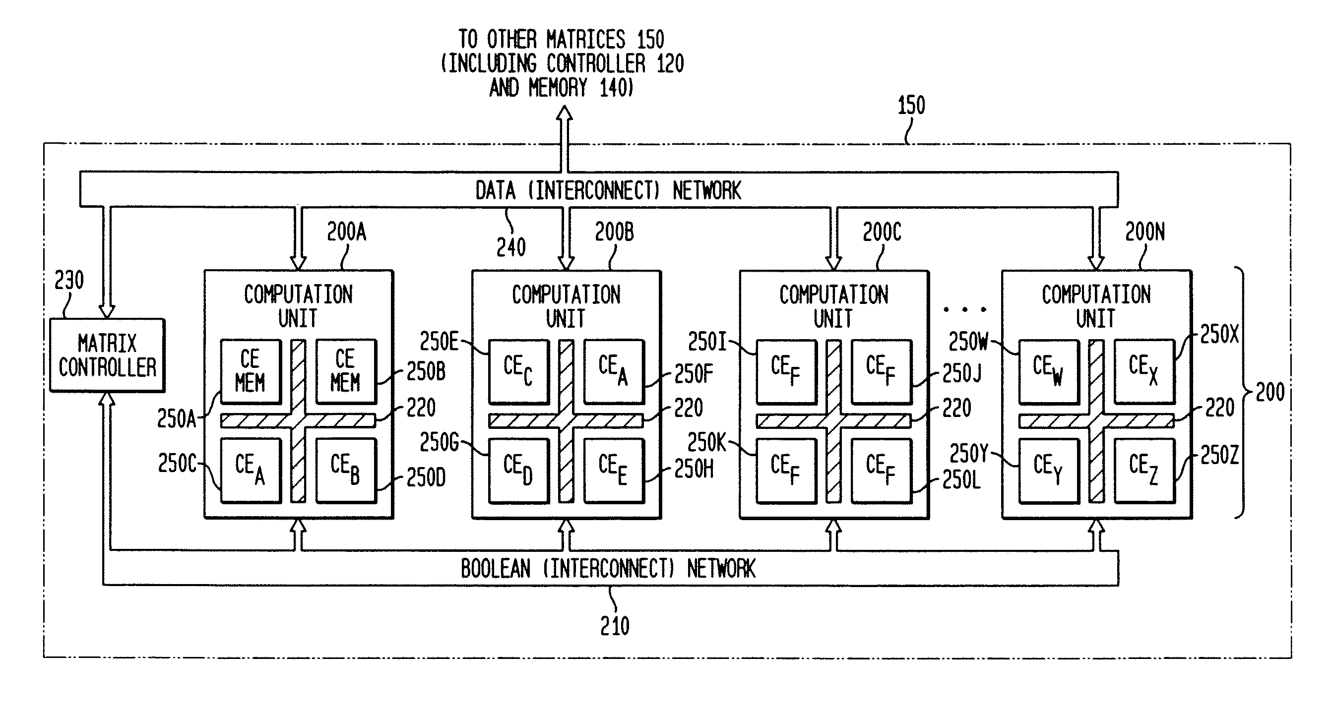
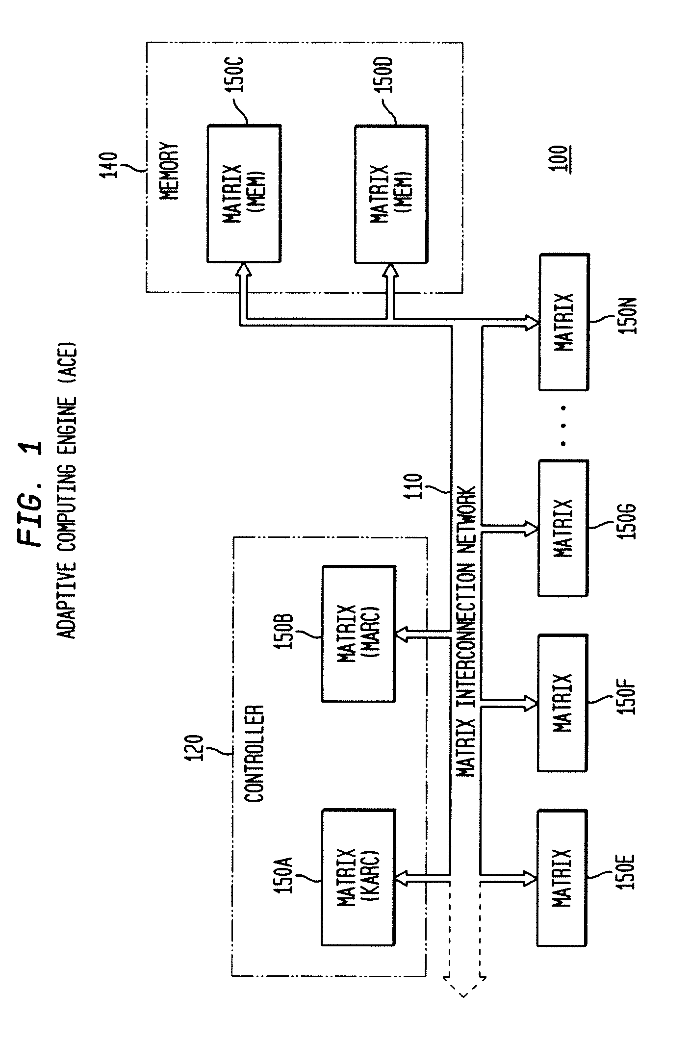
[0029]FIG. 1 is a block diagram illustrating an exemplary apparatus 100 embodiment in accordance with the present invention. The apparatus 100, ...


PUM


Abstract

The present invention concerns a new category of integrated circuitry and a new methodology for adaptive or reconfigurable computing. The exemplary IC embodiment includes a plurality of heterogeneous computational elements coupled to an interconnection network. The plurality of heterogeneous computational elements include corresponding computational elements having fixed and differing architectures, such as fixed architectures for different functions such as memory, addition, multiplication, complex multiplication, subtraction, configuration, reconfiguration, control, input, output, and field programmability. In response to configuration information, the interconnection network is operative in real-time to configure and reconfigure the plurality of heterogeneous computational elements for a plurality of different functional modes, including linear algorithmic operations, non-linear algorithmic operations, finite state machine operations, memory operations, and bit-level manipulations. The various fixed architectures are selected to comparatively minimize power consumption and increase performance of the adaptive computing integrated circuit, particularly suitable for mobile, hand-held or other battery-powered computing applications. In an exemplary embodiment, some or all of the computational elements are alternately configured to implement two or more functions.

Description

CROSS-REFERENCES TO RELATED APPLICATIONS[0001]This is a continuation-in-part application of U.S. patent application Ser. No. 09 / 815,122 entitled “ADAPTIVE INTEGRATED CIRCUITRY WITH HETEROGENEOUS AND RECONFIGURABLE MATRICES OF DIVERSE AND ADAPTIVE COMPUTATIONAL UNITS HAVING FIXED, APPLICATION SPECIFIC COMPUTATIONAL ELEMENTS,” filed on Mar. 22, 2001, the disclosure of which is hereby incorporated by reference in their entirety as if set forth in full herein for all purposes.BACKGROUND OF THE INVENTION[0002]The present invention relates, in general, to integrated circuits and, more particularly, to adaptive integrated circuitry with heterogeneous and reconfigurable matrices of diverse and adaptive computational units having fixed, application specific computational elements.[0003]The advances made in the design and development of integrated circuits (“ICs”) have generally produced ICs of several different types or categories having different properties and functions, such as the class ...

Claims


Application Information

Patent Timeline
IPC IPC(8): G06F15/00G06F15/78
CPCG06F15/7867G06F15/177Y02B60/1225Y02B60/1207Y02D10/00
Inventor PLUNKETT, ROBERT T.HEIDARI, GHOBADMASTER, PAUL L.
Owner ALTERA CORP
Learn More