Method, system and design structure for symmetrical capacitor

a technology of symmetrical capacitors and capacitors, applied in the direction of semiconductor devices, semiconductor/solid-state device details, electrical equipment, etc., can solve the problems of reduced semiconductor chip area availability for other circuit structures, large chip area footprints of moscap capacitors in integrated circuits, and high production costs

Inactive Publication Date: 2008-05-01
TAIWAN SEMICON MFG CO LTD
View PDF16 Cites 26 Cited by
  • Summary
  • Abstract
  • Description
  • Claims
  • Application Information

AI Technical Summary

Problems solved by technology

However, MOSCAP capacitors generally require large chip area footprints in integrated circuits (IC).
Accordingly, design requirements typically result in requiring large semiconductor chip footprint areas or real estate for MOSCAP capacitor structures relative to their circuit capacitance properties, resulting in high production costs and reduced semiconductor chip area availability for other circuit structures.
Moreover, current leakage during a semiconductor circuit's idle mode is known to result in increased power consumption.
And incorrect polarity usage may cause circuit performance degradation.
Accounting for such polarity issues results in circuit design inefficiencies as additional design time must be expended to distinguish between input and output polarities.
In configurations wherein the capacitors are close to the substrate, the variable extrinsic capacitances between the bottom plates closest to the substrate cannot be adequately controlled for in circuit design, as the value of the extrinsic capacitances may not be precisely predicted.
It also presents other difficulties in providing a symmetrical BEOL capacitor structure created from multiple VNCAP's and MIMCAP's.

Method used


Image

  • Method, system and design structure for symmetrical capacitor
  • Method, system and design structure for symmetrical capacitor
  • Method, system and design structure for symmetrical capacitor

Examples


Embodiment Construction

)

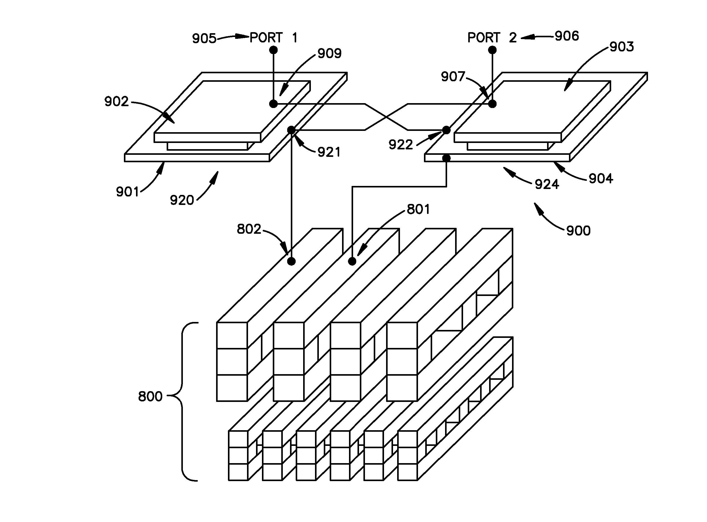
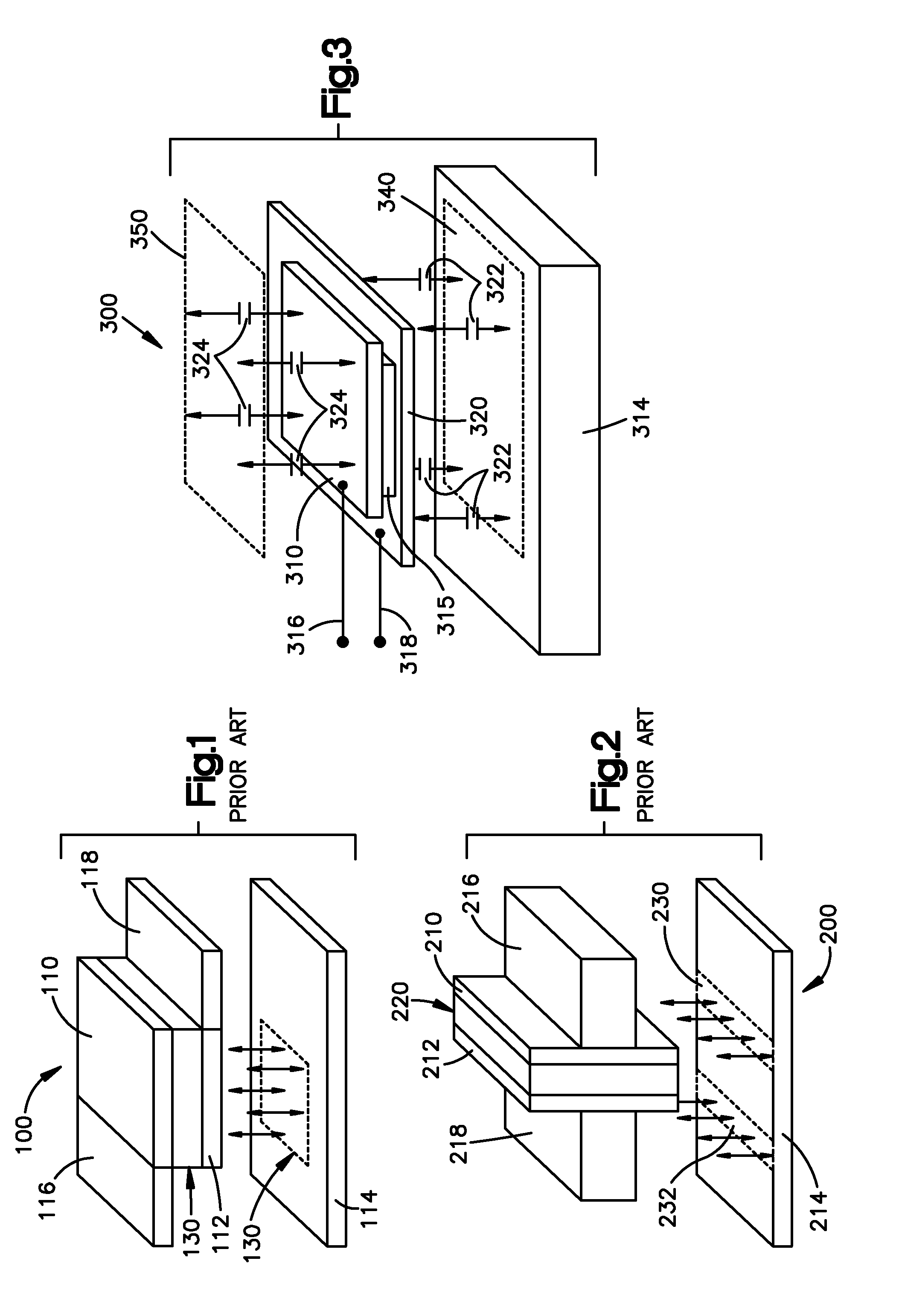
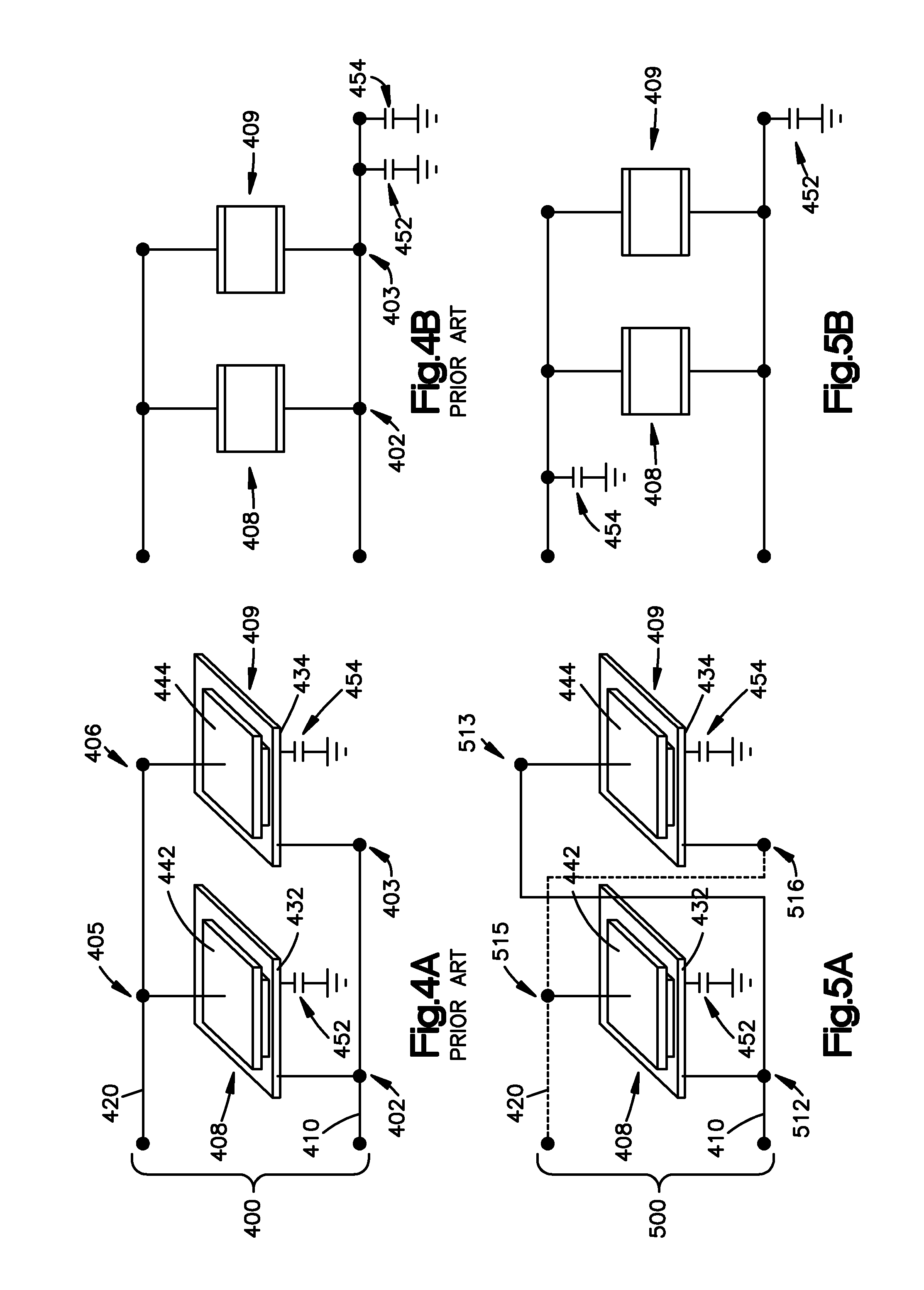
[0035]FIG. 3 illustrates an example of a single asymmetrical BEOL MIMCAP 300 appropriate for use with the present invention, having a top plate 310 and a bottom plate 320 arrayed laterally with respect to a substrate 314 and having connectors or ports 316, 318, respectively. A dielectric material 315 placed between the plates 310, 320 completes a capacitive structure in a lateral plate arrangement with respect to a FEOL substrate 314. (Other FEOL structures are omitted for simplicity of illustration).

[0036] The substrate 314 conventionally is formed of silicon which is dielectric. Preferably, the dielectric material 315 has a permeability value greater than about 4 (er>4). It is to be understood that the plates 310, 320 can be formed of the same material, e.g. polysilicon or copper or other conductive material, or different materials which can be used conventionally for capacitors, depending upon the need and processes.

[0037] The two conductive capacitive plates 310, 320 are moun...


PUM


Abstract

Methods, articles and design structures for capacitance circuits are provided disposing a lower vertical-native capacitor metal layer above a planar front-end-of-line semiconductor base substrate, planar metal bottom plates spaced a bottom plate distance from the base and top plates above the bottom plates spaced a top plate distance from the base defining metal-insulator-metal capacitors, top plate footprints disposed above the base substrate smaller than bottom plate footprints and exposing bottom plate remainder upper lateral connector surfaces; disposing parallel positive port and negative port upper vertical-native capacitor metal layers over and each connected to top plate and bottom plate upper remainder lateral connector surface. Moreover, electrical connecting of the first top plate and the second bottom plate to the positive port metal layer and of the second top plate and the first bottom to the negative port metal layer impart equal total negative port and positive port metal-insulator-metal capacitor extrinsic capacitance.

Description

CROSS REFERENCE TO RELATED APPLICATION [0001] This application is a continuation-in-part of application Ser. No. 11 / 436,251, filed May 28, 2006.TECHNICAL FIELD [0002] This invention relates generally to methods, systems and design structures, and more specifically for capacitors and capacitor structures with symmetrical characteristics. BACKGROUND ART [0003] On-chip capacitors are critical components of integrated circuits that are fabricated on silicon semiconductors. These capacitors are used for a variety of purposes: illustrative examples include bypass and capacitive matching as well as coupling and decoupling. The design and implementation of capacitor structures on silicon semiconductor chips may be dependent upon one or more symmetrical structural, target circuit quality and low parasitic resistance performance characteristics. [0004] More particularly, capacitor structures may be categorized as being formed in one of two regions: the Front End Of (production) Line (FEOL), o...

Claims


Application Information

Patent Timeline
Patent Type & Authority Applications(United States)
IPC IPC(8): H01L29/92H01L21/02
CPCH01L23/5223H01L27/0805H01L29/94H01L2924/0002H01L2924/00
Inventor CHO, CHOONGYEUNKIM, JONGHAEKIM, MOO J.PLOUCHART, JEAN-OLIVIERTRZCINSKI, ROBERT E.
Owner TAIWAN SEMICON MFG CO LTD
Why Eureka
Try Eureka