Method of forming copper wiring in semiconductor device

Inactive Publication Date: 2008-05-01
SK HYNIX INC
View PDF11 Cites 2 Cited by
  • Summary
  • Abstract
  • Description
  • Claims
  • Application Information

AI Technical Summary

Benefits of technology

[0009]Embodiments of the present invention are directed to a method of forming a copper wiring, which is capable of preventing a complication of a process and an increase in process cost.
[0010]Further, embodiments of the present invention are directed to a method of forming a copper wiring, which is capable of preventing a reduction in a polishing uniformity.
[0011]Also, embodiments of the present invention are directed to a method of forming a copper wiring, which is capable of preventing occurrence of a dishing.
[0012]In addition, embodiments of the present invention are directed to a method of forming a copper wiring, which is capable of preventing reduction in a polishing speed.

Problems solved by technology

When forming a copper wiring using the damascene process as known conventionally, disadvantages exist in that separate CMP processes are required for polishing the copper and polishing the barrier metal film, thereby increasing the complexity of the process and the cost involved.
In addition, because the CMP process is performed twice, the layers or films on the semiconductor substrate may be unevenly polished and even the layers or films on different substrates undergoing the polishing process may be unevenly polished with respect to other substrates when the conventional method of forming a copper wiring using the damascene process is used.
Further, the conventional method of forming a copper wiring using the damascene process has a disadvantage in that a dishing of the copper wiring can easily occur as a result of an over polishing for removing copper residue.
However, there is a disadvantage that polishing ununiformity is increased due to the reduction in a polishing speed because the polishing speed is slow in the ultra low pressure polishing.

Method used


Image

  • Method of forming copper wiring in semiconductor device
  • Method of forming copper wiring in semiconductor device
  • Method of forming copper wiring in semiconductor device

Examples


Embodiment Construction

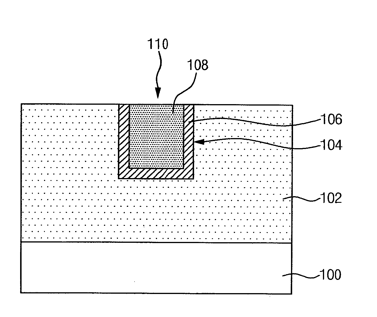
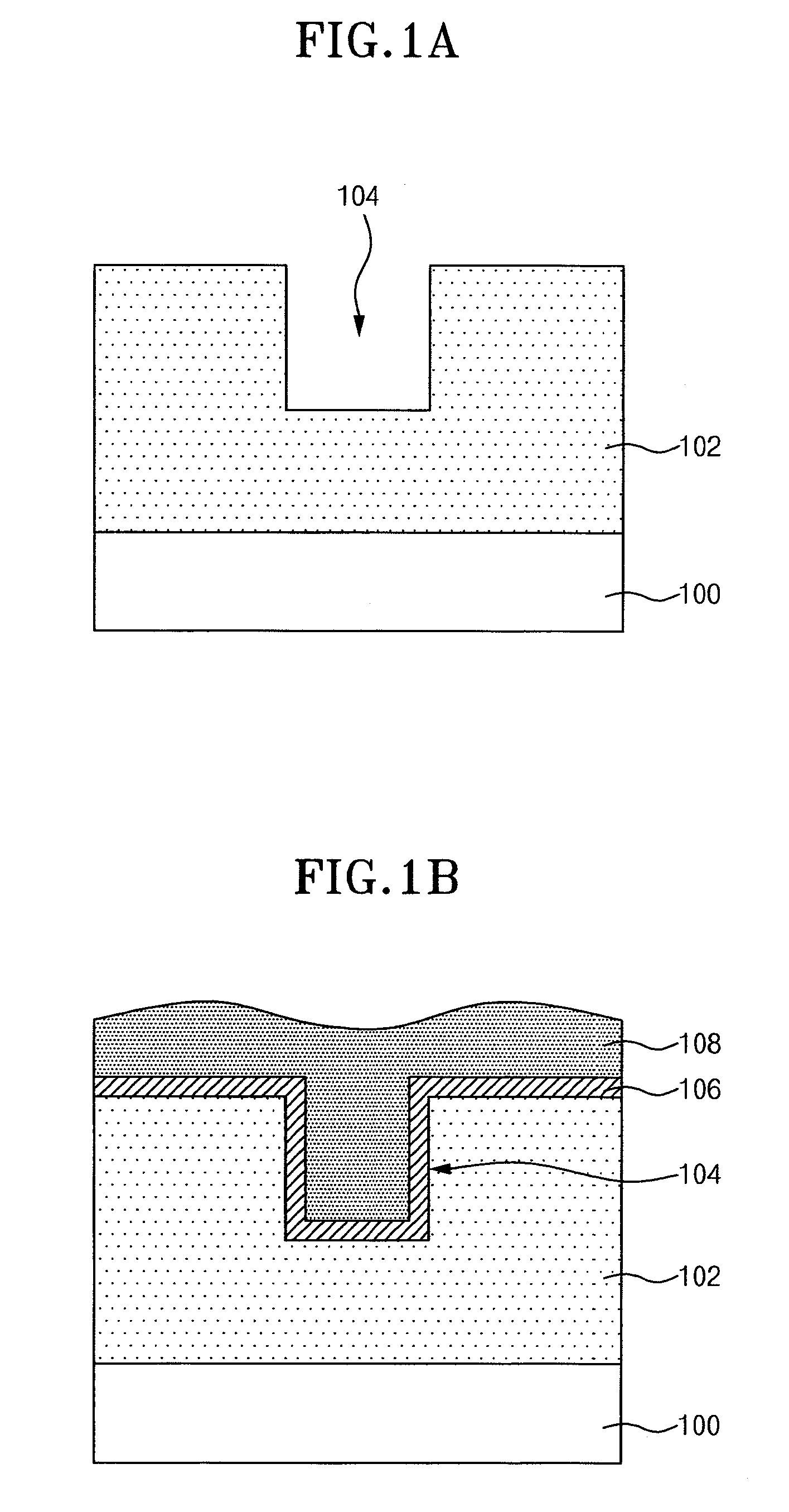
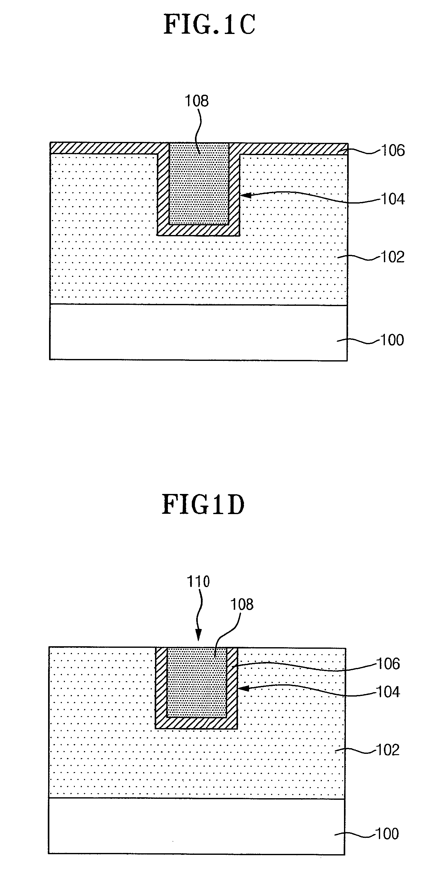
[0028]A preferred embodiment of the present invention is directed to a method of forming a copper wiring, in which a polishing for a copper film and a barrier metal film is performed in an electrochemical mechanical polishing which applies an electric field while supplying abrasive free slurry on a fixed-abrasive pad in which the abrasive particles are fixedly bonded to a pad.

[0029]Therefore, in an embodiment of the present invention, since the slurry without the abrasive particles is used, an over polishing required to remove slurry residue can be reduced and thus it can be possible to proceed a defect free process capable of restricting a dishing. Further, in an embodiment of the present invention, because it is not necessary to use another slurry for polishing a barrier metal film after polishing a copper film, it is possible to prevent complication in process and cost increase and, particularly, it is possible to reduce polishing ununiformity since it is possible to polish both ...


PUM


Abstract

A semiconductor package includes method of forming a copper wiring may comprise forming an interlayer insulation film provided with a damascene pattern for wiring over a semiconductor substrate; depositing a barrier metal film over a surface of the damascene pattern and the interlayer insulation film; depositing a copper film over the barrier metal film so as to fill the damascene pattern; and performing an electrochemical mechanical polishing by using a fixed-abrasive pad, supplying an electrolyte solution, and applying an electric field so as to expose the interlayer insulation film.

Description

CROSS-REFERENCE TO RELATED APPLICATIONS[0001]The present application claims priority to Korean patent application number 10-2006-0106908 filed on Oct. 31, 2006, which is incorporated herein by reference in its entirety.BACKGROUND OF THE INVENTION[0002]The present invention relates to a method of forming a copper wiring in a semiconductor device, and more particularly to a method of forming a copper wiring capable of preventing a reduction in a polishing speed and a reduction in a polish uniformity.[0003]Because it is difficult to etch copper by a conventional etching process, a damascene process is generally used to form a copper wiring. Hereinafter, a conventional method of forming a copper wiring using the damascene process will be briefly described.[0004]After an interlayer insulation film is formed over an upper portion of a semiconductor substrate, the interlayer insulation film is etched to form a damascene pattern consisting of a hole or a hole and a trench for wiring. After ...

Claims


Application Information

Patent Timeline
IPC IPC(8): H01L21/4763
CPCH01L21/32125H01L21/3205H01L21/304
Inventor RYU, CHEOL HWIPARK, HYUNG SOONSHIN, JONG HANPARK, JUM YONGKIM, SUNG JUN
Owner SK HYNIX INC
Why Eureka
Try Eureka