Method for manufacturing electronic substrate

a technology of electronic substrates and manufacturing methods, applied in the direction of sustainable manufacturing/processing, final product manufacturing, printed circuit non-printed electric components association, etc., can solve the problems of reducing adhesive strength, and affecting the effect of adhesive strength

Active Publication Date: 2008-05-08
SEIKO EPSON CORP
View PDF9 Cites 17 Cited by
  • Summary
  • Abstract
  • Description
  • Claims
  • Application Information

AI Technical Summary

Benefits of technology

[0009]An advantage of the present invention is to provide a method for manufacturing an electronic substrate, by which electronic components are stably mounted and secured.
[0010]According to an aspect of the invention, a method for manufacturing an electronic substrate including an electronic component bonded with adhesive to a base part, the method includes (a) applying a droplet containing the adhesive to an area on the base part, the area facing to the electronic component, within a range substantially equal to a size of the electronic component by using a droplet ejection head moving in relatively to the base part, and (b) mounting the electronic component on the adhesive applied to the base part.
[0011]In this manner, the droplet containing the adhesive is applied to an area on the base part, within a range substantially equal to a size of the electronic component, thereby preventing air from being trapped between the mounted electronic component and the base part. It is therefore possible to prevent cracks from appearing due to expansion of the air or the like even in the case of heat application for the purpose of curing the adhesive. Thus, the electronic component maintains stable adhesive strength.
[0012]In this manner, the droplet containing the adhesive is applied by a droplet ejection system, which makes it easy to pattern the adhesive without use of a mask or a photoresist, which is used in a printing method or a photolithographic method, and prevents the adhesive from being wasted, thereby being able to contribute to reduced cost.
[0013]In the above-mentioned method, it is preferable that the applied adhesive be brought in a half-cured state before the step (b).
[0014]In this manner, the electronic component is easily mounted on the adhesive in a half-cured state, thereby bringing the electronic component into intimate contact with the adhesive, leading to improvement in adhesiveness. The electronic component is buried in the adhesive depending on viscosity of the applied adhesive or pressure for mounting the electronic component. Thus, side surfaces of the electronic component are brought into intimate contact with the adhesive to enhance adhesion strength. Furthermore, in the case where the adhesive contracts by heat, the contraction force functions as force for holding the electronic component, thereby enhancing more adhesion strength.

Problems solved by technology

The related art such as described above, however, has a following problem.
However, where the electronic components are mounted on the adhesive applied in this manner, the adhesive spreads but not enough to fill out each space between the electronic components and the base part, thereby causing gaps therebetween in many cases.
In this case, there is a problem in that air remaining in the gaps may expand during heating for curing the adhesive, thereby causing cracks in the cured adhesive, which decrease adhesive strength.

Method used


Image

  • Method for manufacturing electronic substrate
  • Method for manufacturing electronic substrate
  • Method for manufacturing electronic substrate

Examples


Embodiment Construction

[0040]Hereinafter, an embodiment of a method for manufacturing an electronic substrate in accordance with this embodiment will be explained with reference to FIGS. 1 to 5C.

[0041]Each element is set in a recognizable size by changing a reduction scale as needed in each drawing referenced below.

Droplet Ejection Device

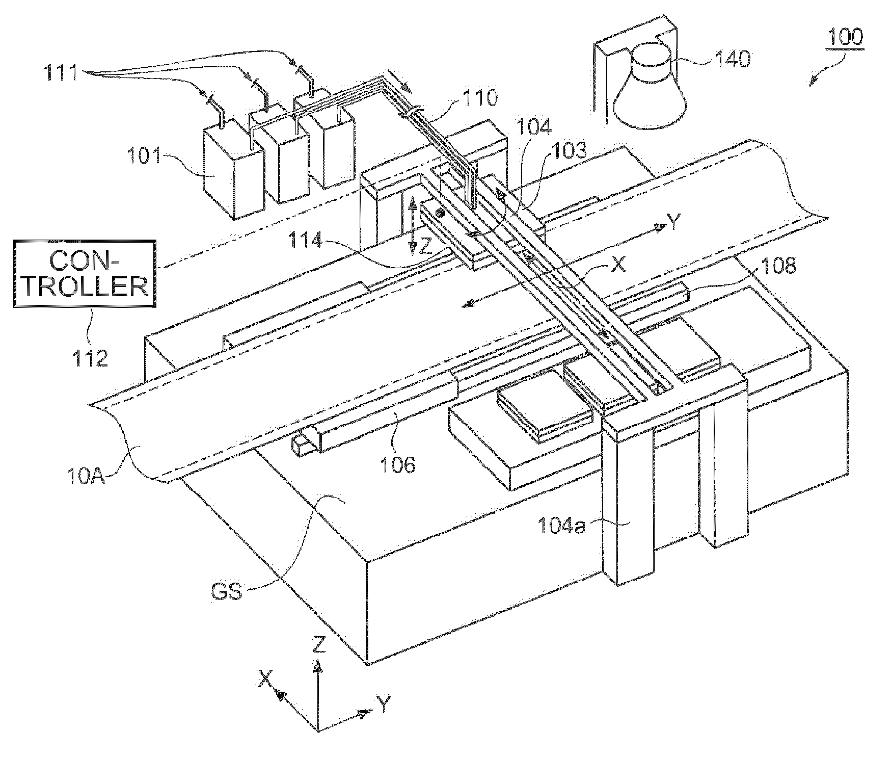
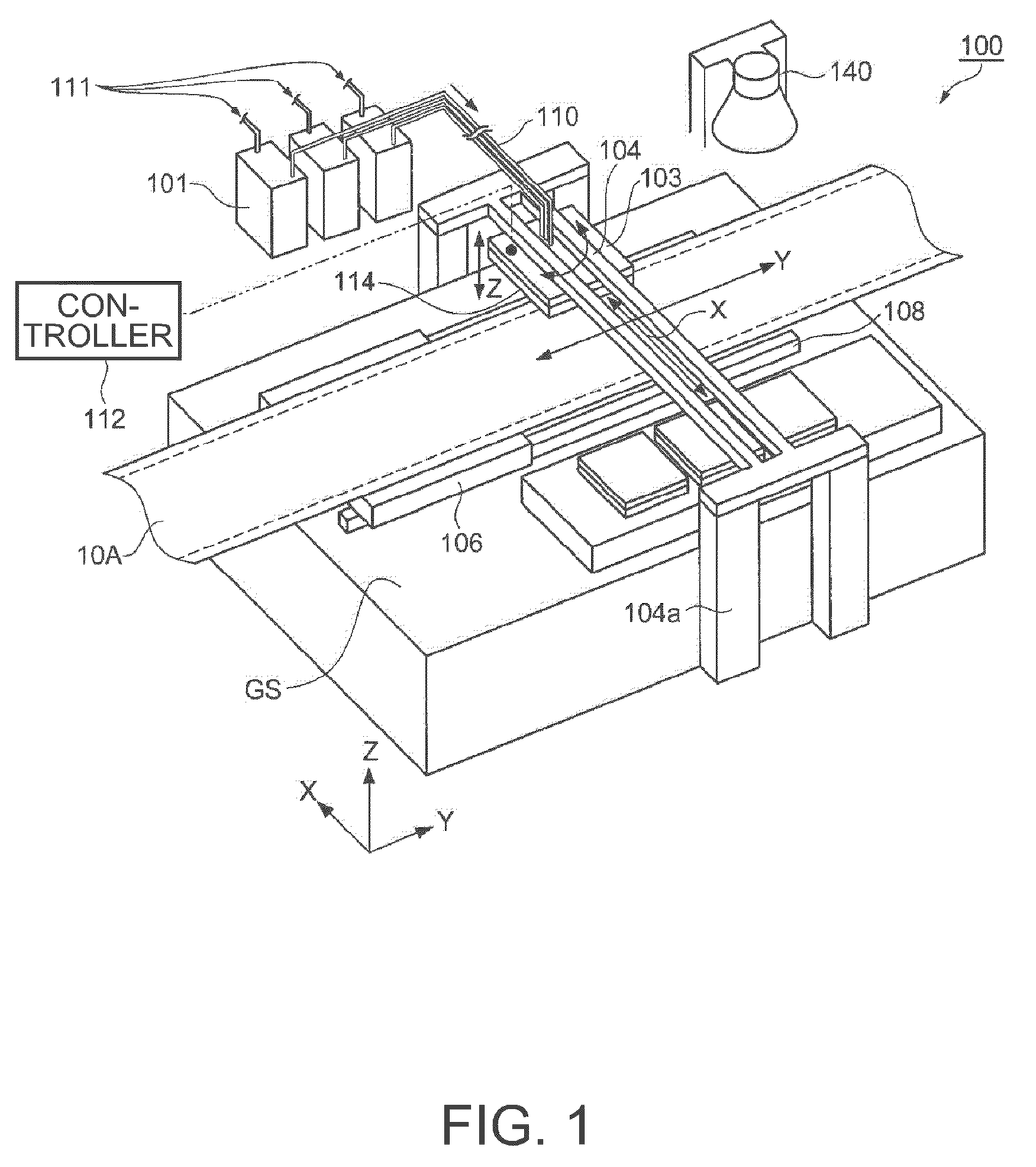
[0042]First described is a droplet ejection device used in the method for manufacturing the electric substrate in accordance with this invention, with reference to FIGS. 1 to 2B.

[0043]A droplet ejection device 1 shown in FIG. 1 is basically an inkjet device. To be more specific, the droplet ejection device 1 includes tanks 101 holding fluid material 111, tubes 110, a ground stage GS, an ejection head unit (a droplet ejection head unit) 103, a stage 106, a first position controller 104, a second position controller 108, a controller 112, a light irradiation device 140, and supporters 104a.

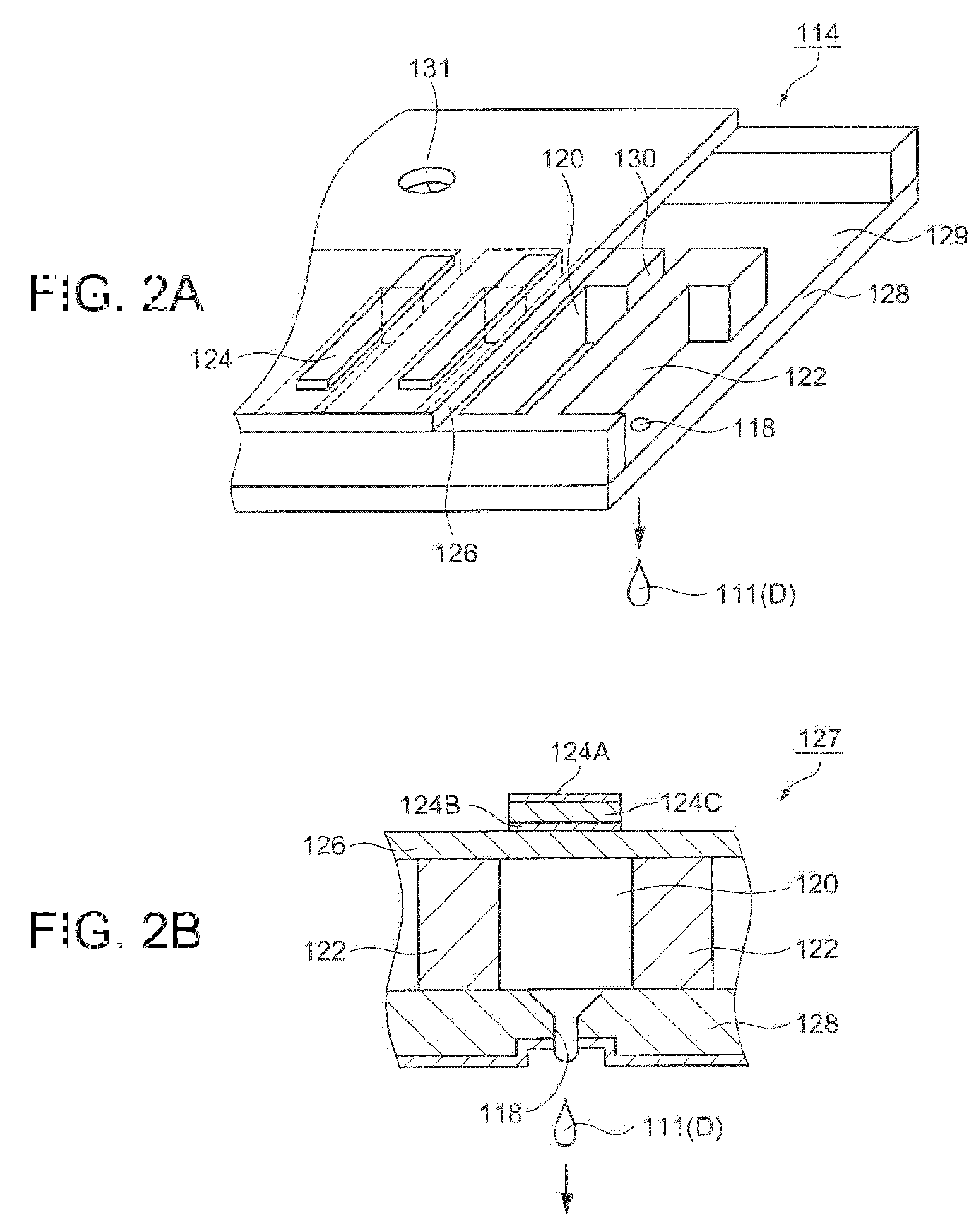
[0044]The ejection head unit 103 holds a head 114 shown in FIG. 2A. The head 114 eje...


PUM

PropertyMeasurementUnit
diameteraaaaaaaaaa
volumeaaaaaaaaaa
volumeaaaaaaaaaa

Abstract

A method for manufacturing an electronic substrate including an electronic component bonded with adhesive to a base part, comprises (a) applying a droplet containing the adhesive to an area on the base part, the area facing to the electronic component, within a range substantially equal to a size of the electronic component by using a droplet ejection head moving in relatively to the base part, and (b) mounting the electronic component on the adhesive applied to the base part.

Description

BACKGROUND OF THE INVENTION[0001]1. Technical Field[0002]The present invention relates to a method for manufacturing an electronic substrate.[0003]2. Related Art[0004]As electronic substrates grow more sophisticated and smaller, the demand for more integration and more functionality of electronic substrates mounted with electronic components such as IC chips has become stronger in recent years.[0005]JA-A-3-69191 is an example of related art, in which an electronic substrate is manufactured by mounting electronic components on copper wirings formed on a substrate member, coating a surface with resins at once to constitute an electronic component buried layer, and then laminating the thusly achieved electronic component buried layer using an adhesive.[0006]The related art such as described above, however, has a following problem.[0007]The above electronic component is generally secured with adhesive to a base part on which the electronic component is to be mounted. This adhesive is ap...

Claims


Application Information

Patent Timeline
Patent Type & Authority Applications(United States)
IPC IPC(8): H05K3/30H05K1/16H05K3/10B32B37/00
CPCB32B37/1292Y10T29/4913B32B2309/04B32B2310/0831B32B2457/00H01L24/24H01L24/82H01L24/83H01L2224/24011H01L2224/24226H01L2224/76155H01L2224/83192H01L2224/83855H01L2924/01005H01L2924/01015H01L2924/01029H01L2924/01047H01L2924/01082H01L2924/07802H01L2924/14H01L2924/19041H01L2924/19043H05K1/185H05K3/125H05K3/305H05K3/4664H05K2201/10636H05K2201/10674H05K2203/013H01L24/29H01L2224/2919H01L2924/01006H01L2924/01033H01L2924/0665B32B2309/02Y10T29/49144Y10T29/49128Y10T29/49126Y10T29/49155H01L2224/82102H01L2224/743H01L24/743H01L2924/00H01L2924/3512H01L2224/04105H01L2224/27848H01L2224/73267H01L2224/83048H01L2224/83874H01L2224/92244H01L2924/12044Y02P70/50H05K1/18
Inventor SHINTATE, TSUYOSHI
Owner SEIKO EPSON CORP
Why Eureka
Try Eureka