Vertical Integration of Passive Component in Semiconductor Device Package for High Electrical Performance

a technology of passive components and semiconductor devices, applied in semiconductor devices, semiconductor/solid-state device details, electrical apparatus, etc., can solve the problems of reducing area and attempting to increase density, and reaches the practical limit, so as to reduce noise, improve performance, and reduce area

Inactive Publication Date: 2008-05-08
TEXAS INSTR INC
View PDF4 Cites 2 Cited by
  • Summary
  • Abstract
  • Description
  • Claims
  • Application Information

AI Technical Summary

Benefits of technology

[0015]The invention has advantages including but not limited to one or more of the following: providing manufacturing methods for high-performance semiconductor device package systems; providing package assemblies having reduced area; reduced susceptibility to noise; improved performance; and reduced manufacturing costs. These and other features, advantages, and benefits of the present invention can be understood by one of ordinary skill in the arts upon careful consideration of the detailed description of representative embodiments of the invention in connection with the accompanying drawings.

Problems solved by technology

Efforts are continuously being made to design and manufacture devices with reduced area, but attempts to increase density while reducing area eventually reach a practical limit.
In addition to the need for a reduction in the area occupied by ICs and associated passive components, other related problems concern performance.

Method used


Image

  • Vertical Integration of Passive Component in Semiconductor Device Package for High Electrical Performance
  • Vertical Integration of Passive Component in Semiconductor Device Package for High Electrical Performance
  • Vertical Integration of Passive Component in Semiconductor Device Package for High Electrical Performance

Examples


Embodiment Construction

[0025]The invention provides high-performance semiconductor package systems and methods related to their manufacture. The vertical integration of passive circuit components into packages which also include more sophisticated ICs provides package systems having a reduced overall footprint and superior electrical performance.

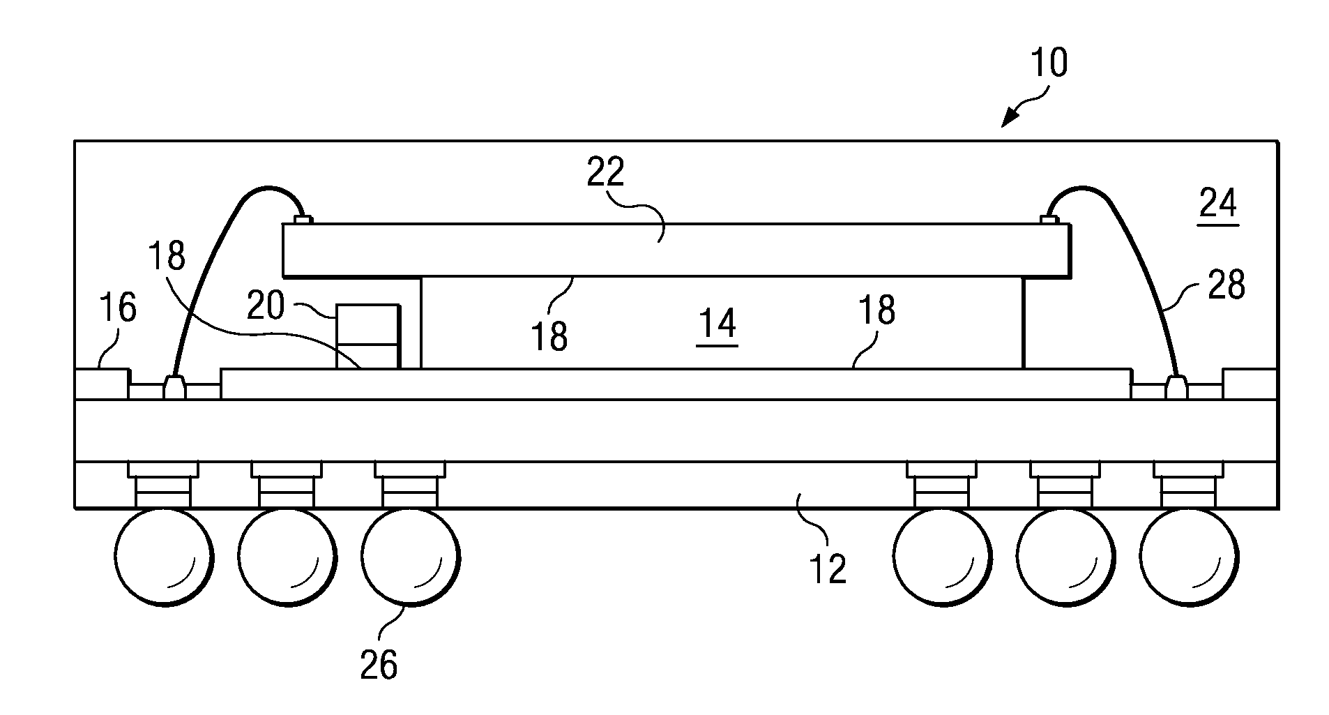
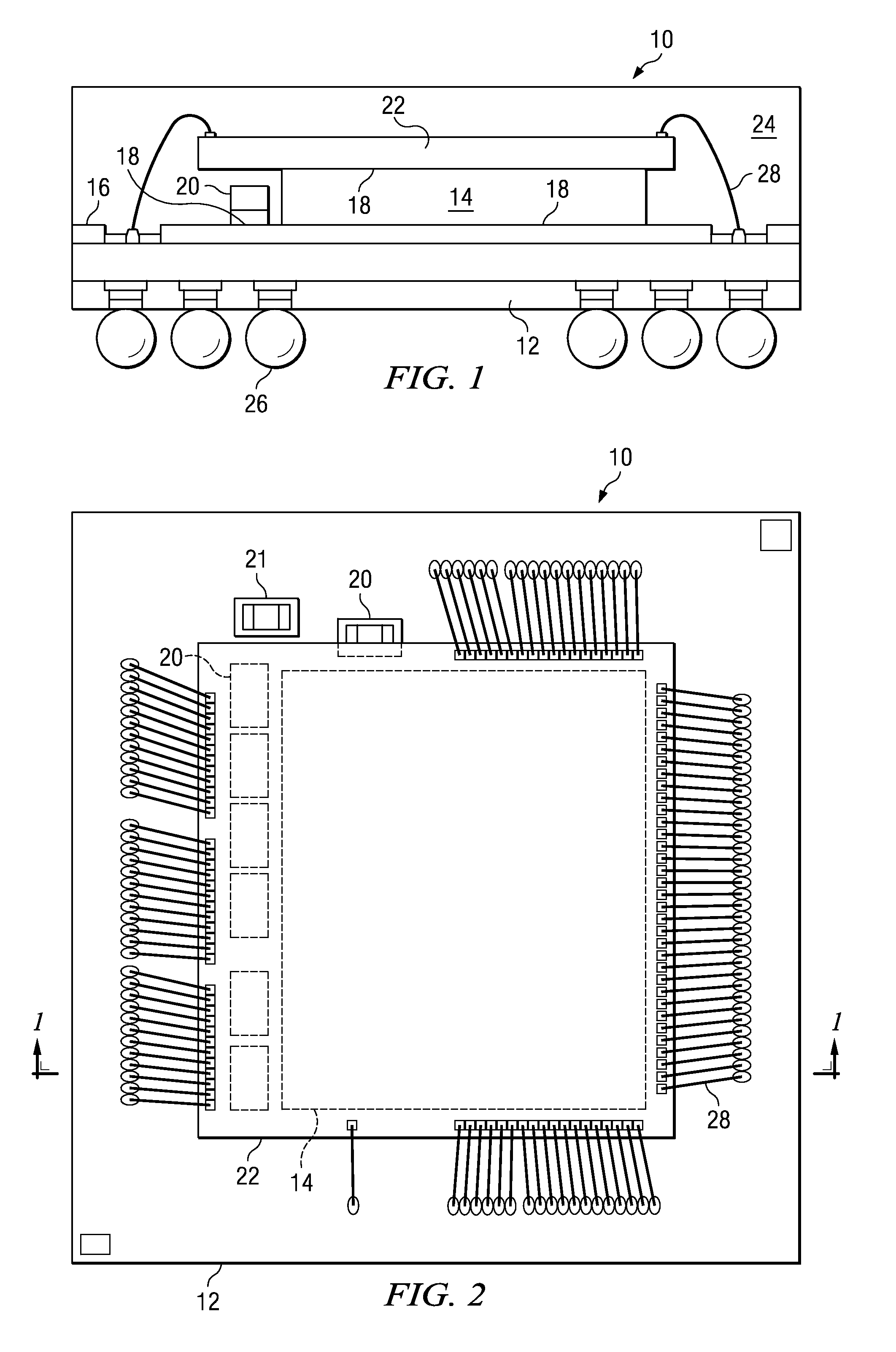
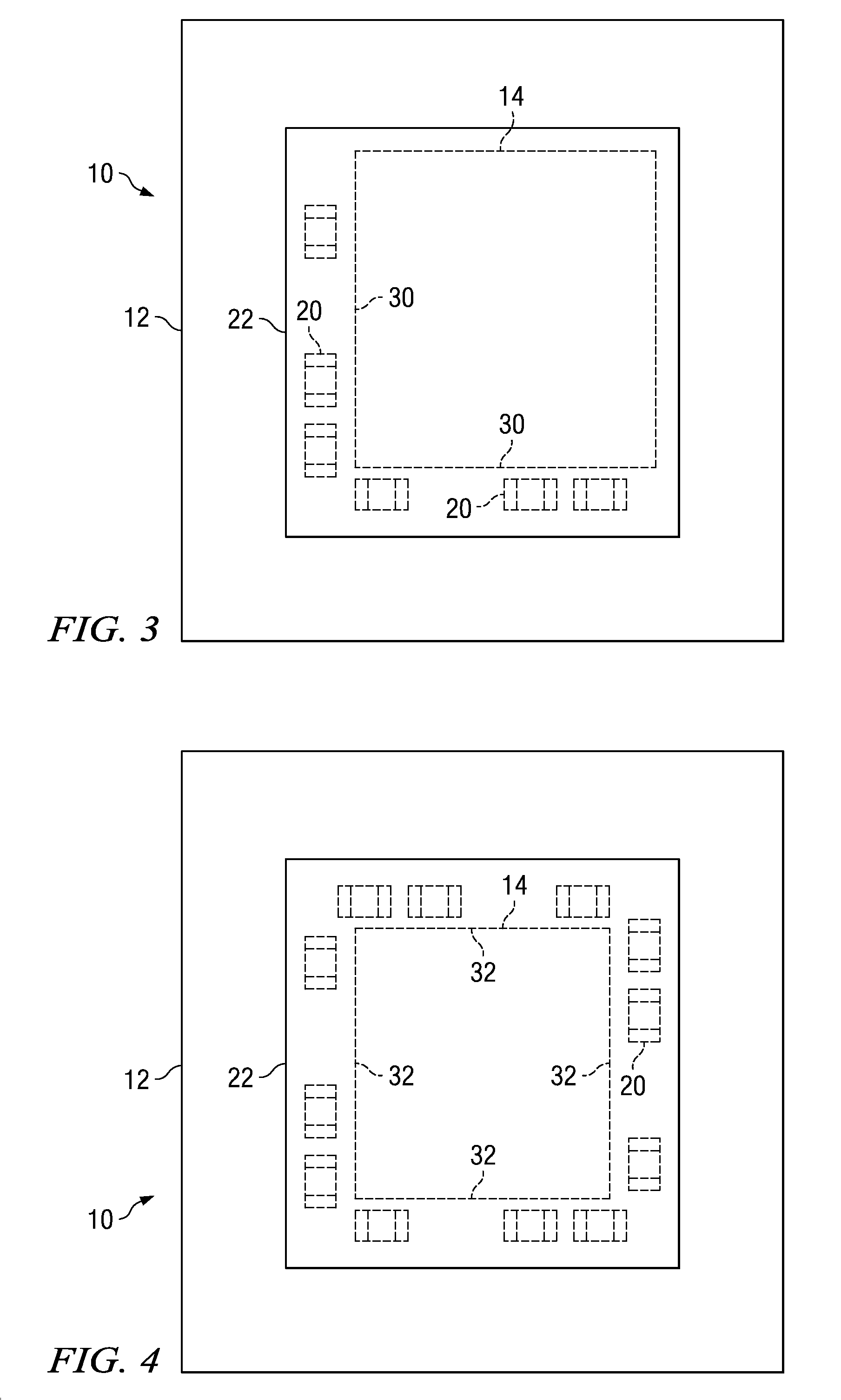
[0026]First referring primarily to FIG. 1, a cutaway side view shows an exemplary embodiment of a semiconductor device package system 10 of the invention. A substrate 12 such as a multi-layer PCB suitable for a fine pitch PBGA for example, is shown with a spacer 14 affixed to one of its surfaces 16 with die attach material 18 such as die attach film or curable die attach adhesive known in the arts. Adjacent to the spacer 14, one or more passive circuit components 20 are affixed to the substrate 12 surface 16, preferably using similar or identical die attach material 18. A chip 22, preferably an integrated circuit relatively large and complex relative to the passiv...


PUM


Abstract

A high performance package and methods for its assembly are disclosed. A semiconductor package system of the invention is assembled in a method including the steps of affixing one or more spacers to a package substrate and affixing one or more passive components to the substrate adjacent to the spacers in order to define a plane. A semiconductor chip is affixed in the plane atop the one or more passive components and spacers and is electrically coupled to the one or more passive components.

Description

PRIORITY ENTITLEMENT[0001]This application claims priority based on Provisional Patent Application Ser. No. 60 / 863,999 filed on Nov. 2, 2006, which is incorporated herein for all purposes by this reference. This application and the Provisional Patent Application have a common inventor and are assigned to the same entity.TECHNICAL FIELD[0002]The invention relates to electronic semiconductor devices and manufacturing. More particularly, the invention relates to microelectronic semiconductor assemblies having vertically stacked ICs (integrated circuits) and passive circuit components contained within a single package and to methods related to the manufacture of such package systems.BACKGROUND OF THE INVENTION[0003]It is often desirable to include passive components in a semiconductor device package to work in concert with a more complex IC. Commonly, one or more passive components, such as capacitors for example, are mounted on a substrate, such as a PCB (printed circuit board), adjace...

Claims


Application Information

Patent Timeline
Patent Type & Authority Applications(United States)
IPC IPC(8): H01L23/043H01L21/58
CPCH01L23/16H01L23/3128H01L2924/014H01L2924/01033H01L24/48H01L2924/19105H01L24/49H01L25/16H01L2224/32014H01L2224/48091H01L2224/48227H01L2224/48228H01L2224/49171H01L2924/15311H01L2924/19041H01L2924/19103H01L2924/00014H01L2924/00H01L2224/05554H01L2924/10161H01L2924/14H01L2924/181H01L2224/45099H01L2224/05599H01L2924/00012
Inventor TOGAWA, SHINICHI
Owner TEXAS INSTR INC
Why Eureka
Try Eureka