High-Voltage Semiconductor Device and Method of Fabricating the Same

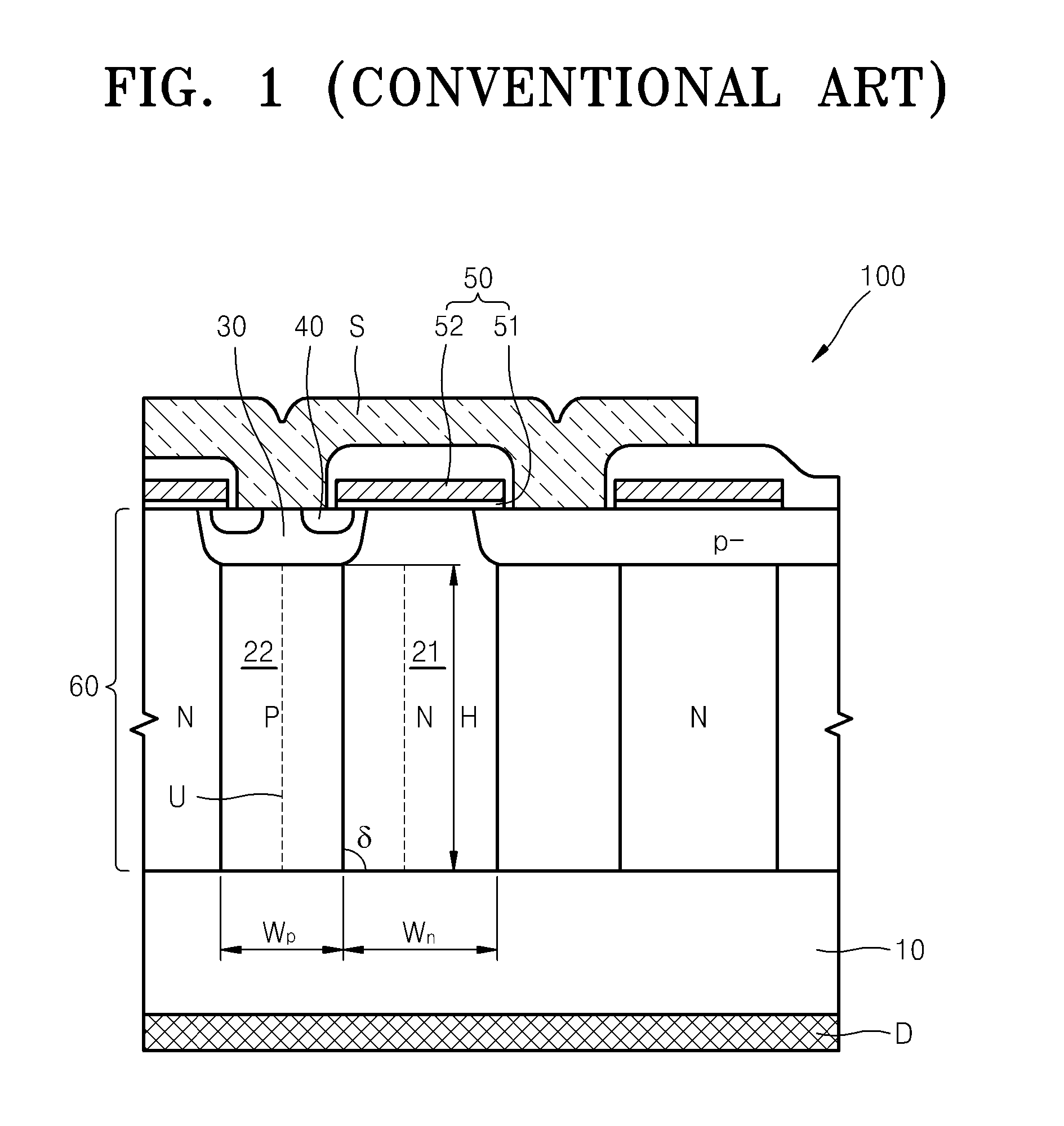
a high-voltage semiconductor and semiconductor technology, applied in semiconductor devices, semiconductor device details, electrical equipment, etc., can solve the problems of difficult to form trenches having precisely vertical sidewalls, lowering the breakdown voltage of high-voltage semiconductor devices, etc., and achieve high breakdown voltage

Active Publication Date: 2008-05-15
SEMICON COMPONENTS IND LLC
View PDF32 Cites 27 Cited by
  • Summary
  • Abstract
  • Description
  • Claims
  • Application Information

AI Technical Summary

Benefits of technology

[0019]In some embodiments of the present invention, the high-voltage semiconductor device may further include a plurality of wells of a second conductivity type disposed adjacent to the top surface of the semiconductor layer, wherein the wells form PN junctions with the charge compensation plugs and the pillars. Also, the high-voltage semiconductor device may further include a plurality of source regions of a first conductivity type dis

Problems solved by technology

However, when the concentration of impurities in the semiconductor body is increased, space charges increase in the semiconductor body thus, lowering the breakdown voltage of the high-voltage semiconductor device.
However, because th

Method used


Image

  • High-Voltage Semiconductor Device and Method of Fabricating the Same
  • High-Voltage Semiconductor Device and Method of Fabricating the Same
  • High-Voltage Semiconductor Device and Method of Fabricating the Same

Examples


Embodiment Construction

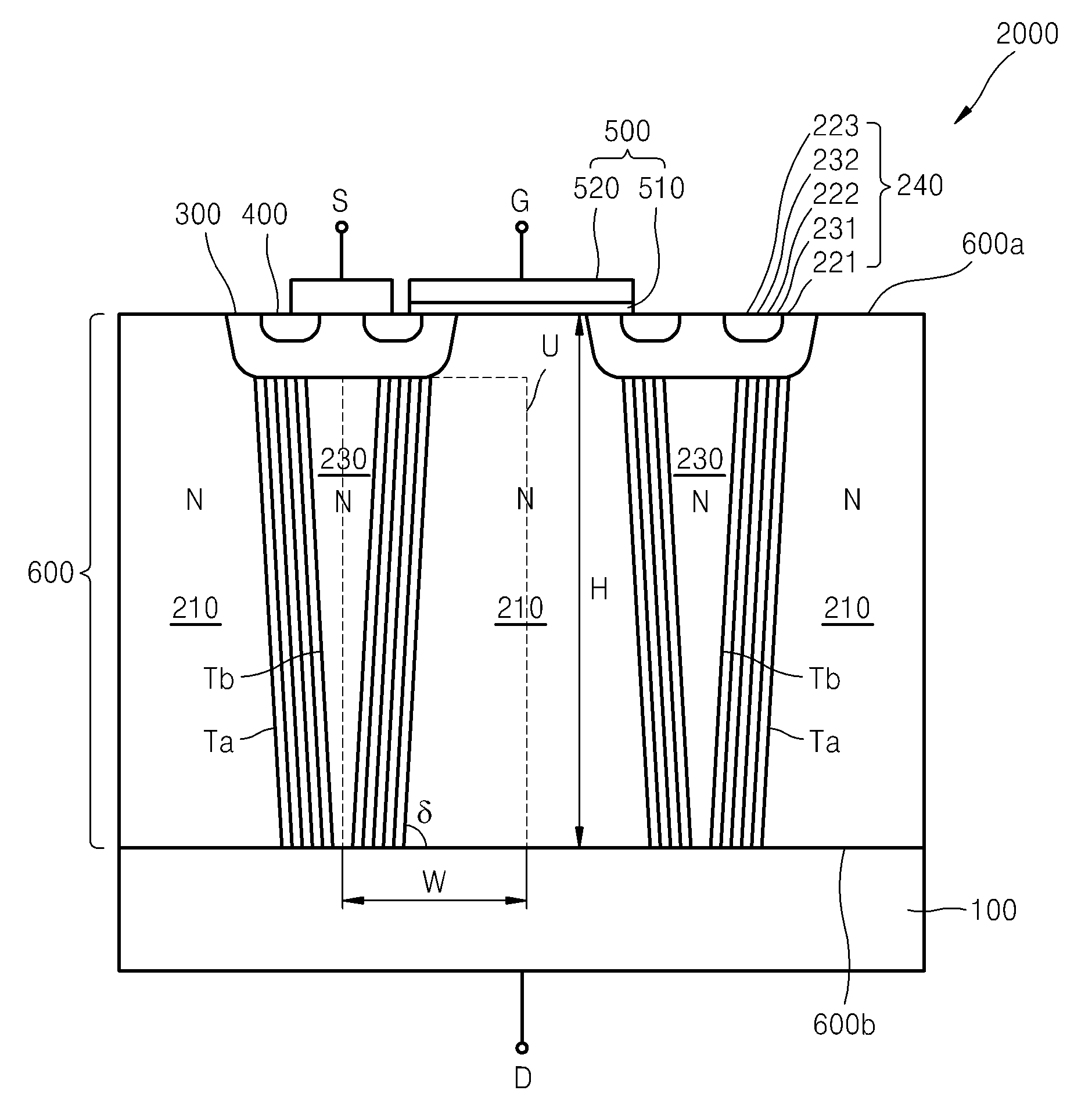
[0032]The present invention will now be described more fully hereinafter with reference to the accompanying drawings, in which exemplary embodiments of the invention are shown. The present invention may, however, be embodied in different forms and should not be construed as limited to the embodiments set forth herein. Rather, these embodiments are provided so that this disclosure is thorough and complete and fully conveys the scope of the invention to one skilled in the art. In the drawings, the thicknesses of layers and regions are exaggerated for clarity. It will also be understood that when a layer is referred to as being “on” another layer or substrate, it can be directly on the other layer or substrate or intervening layers may also be present. The same reference numerals are used to denote the same elements throughout the specification.

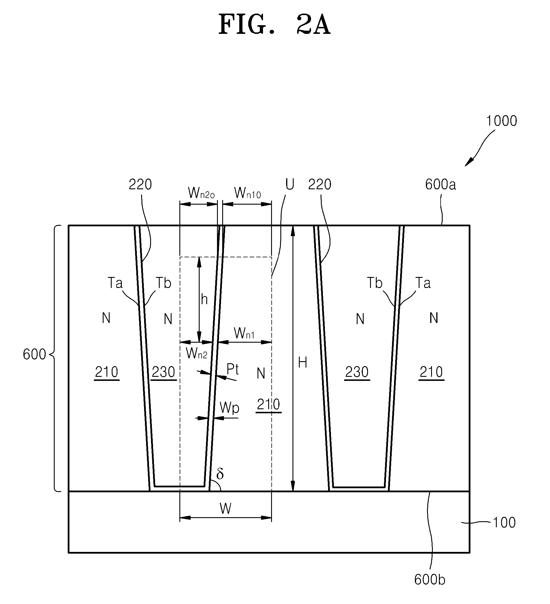
[0033]FIG. 2A is a cross sectional view of a unit superjunction U of a high-voltage semiconductor device 1000 according to an embodiment of the...


PUM


Abstract

A high-voltage semiconductor device includes a semiconductor layer having a plurality of pillars of a first conductivity type defined by a plurality of trenches which extend from a top surface of the semiconductor layer toward a bottom surface thereof. A charge compensation layer of a second conductivity type is disposed over at least sidewalls of each trench to a predetermined thickness to form a groove in each trench. A charge compensation plug of the first conductivity type substantially fills each groove.

Description

CROSS-REFERENCES TO RELATED APPLICATIONS[0001]This application claims priority to the Korean Patent Application No. 10-2006-0113032, filed on Nov. 15, 2006 in the Korean Intellectual Property Office, the disclosure of which is incorporated herein in its entirety by reference.BACKGROUND OF THE INVENTION[0002]The present invention relates to a high-voltage semiconductor device and a method of fabricating the same, and more particularly, to a high-voltage semiconductor device having a superjunction structure that is obtained by alternately forming impurity layers of different types of conductivity.[0003]Conventionally, a high-voltage semiconductor device, such as a power metal oxide semiconductor field effect transistor (MOSFET) or an insulated gate bipolar transistor (IGBT), includes a source region and a drain region that are disposed on a top surface and a bottom surface, respectively, of a semiconductor body. Also, the high-voltage semiconductor device includes a gate insulating la...

Claims


Application Information

Patent Timeline
IPC IPC(8): H01L23/00H01L21/44
CPCH01L29/0634H01L29/0878H01L29/1095H01L29/66333H01L29/66712H01L2924/0002H01L29/7395H01L29/7802H01L2924/00H01L27/06
Inventor LEE, JAE-GILKIM, CHANG-WOOKJANG, HO-CHEOLYUN, CHONG-MAN
Owner SEMICON COMPONENTS IND LLC
Why Eureka
Try Eureka