Semiconductor memory device and write control method thereof

a memory device and write control technology, applied in the direction of information storage, static storage, digital storage, etc., can solve the problems of not having random access, slow access speed of magnetic storage, and small recording capacity to be secured, so as to simplify the control of a semiconductor memory device

Inactive Publication Date: 2008-05-15
LONGITUDE LICENSING LTD
View PDF3 Cites 22 Cited by
  • Summary
  • Abstract
  • Description
  • Claims
  • Application Information

AI Technical Summary

Benefits of technology

[0011]The present invention has been achieved to solve the above problems, and an object of the present invention is to simplify a con

Problems solved by technology

However, the magnetic storage is slow in access speed, and does not have random accessibility in many cases.
However, a recording capacity to be secured is considerably small.
However, the DRAM is a volatile memory, and stored data is lost when the power is turned off.
Thus, the DRAM is not suitable for a program or data to be save for a long period.
Thus, there is a limit to reduction in power consumption, and there is a problem that complicated control by a controller is

Method used


Image

  • Semiconductor memory device and write control method thereof
  • Semiconductor memory device and write control method thereof
  • Semiconductor memory device and write control method thereof

Examples


Embodiment Construction

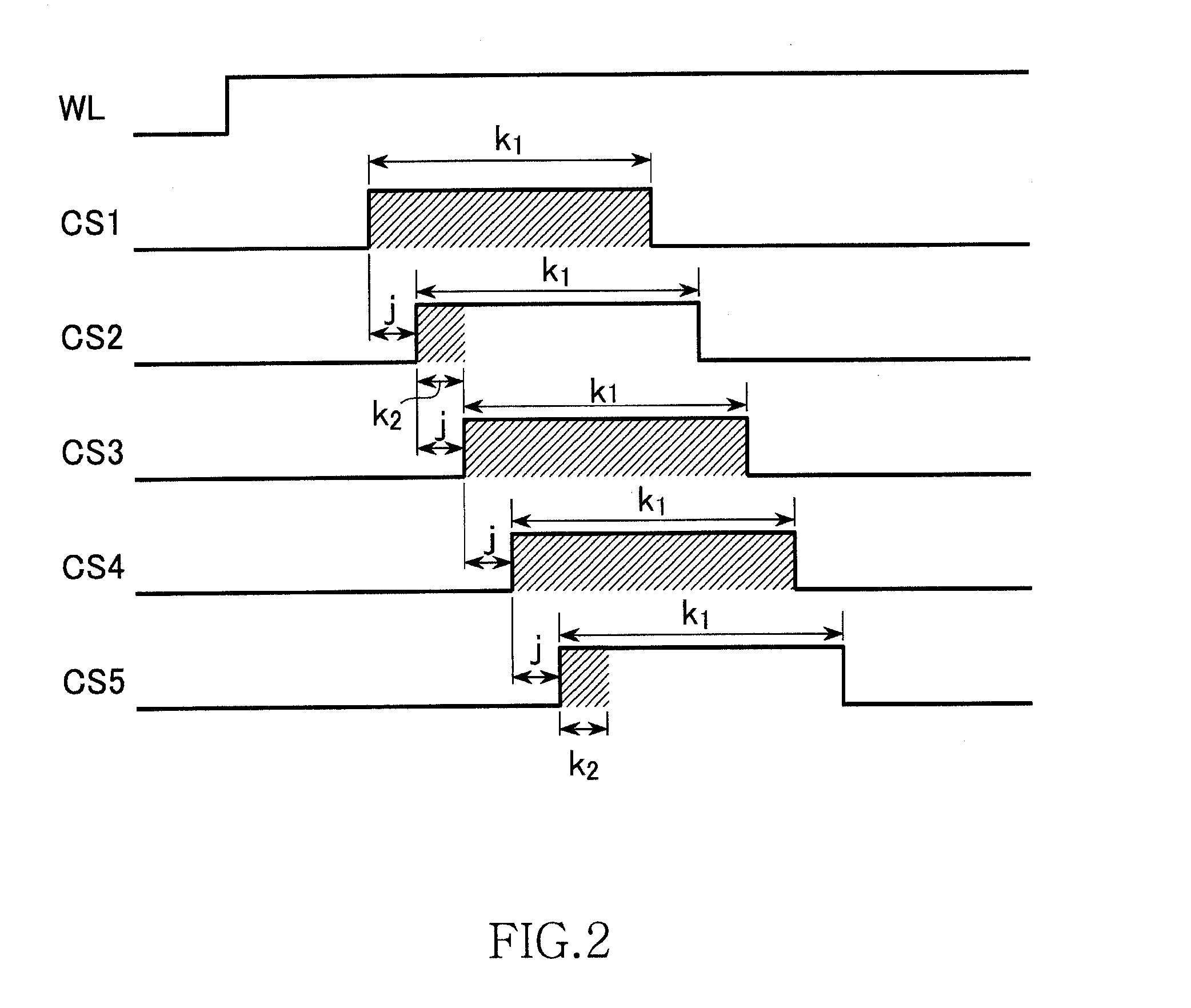
[0036]Before explaining preferred embodiments of the present invention, the principle of the invention is explained.

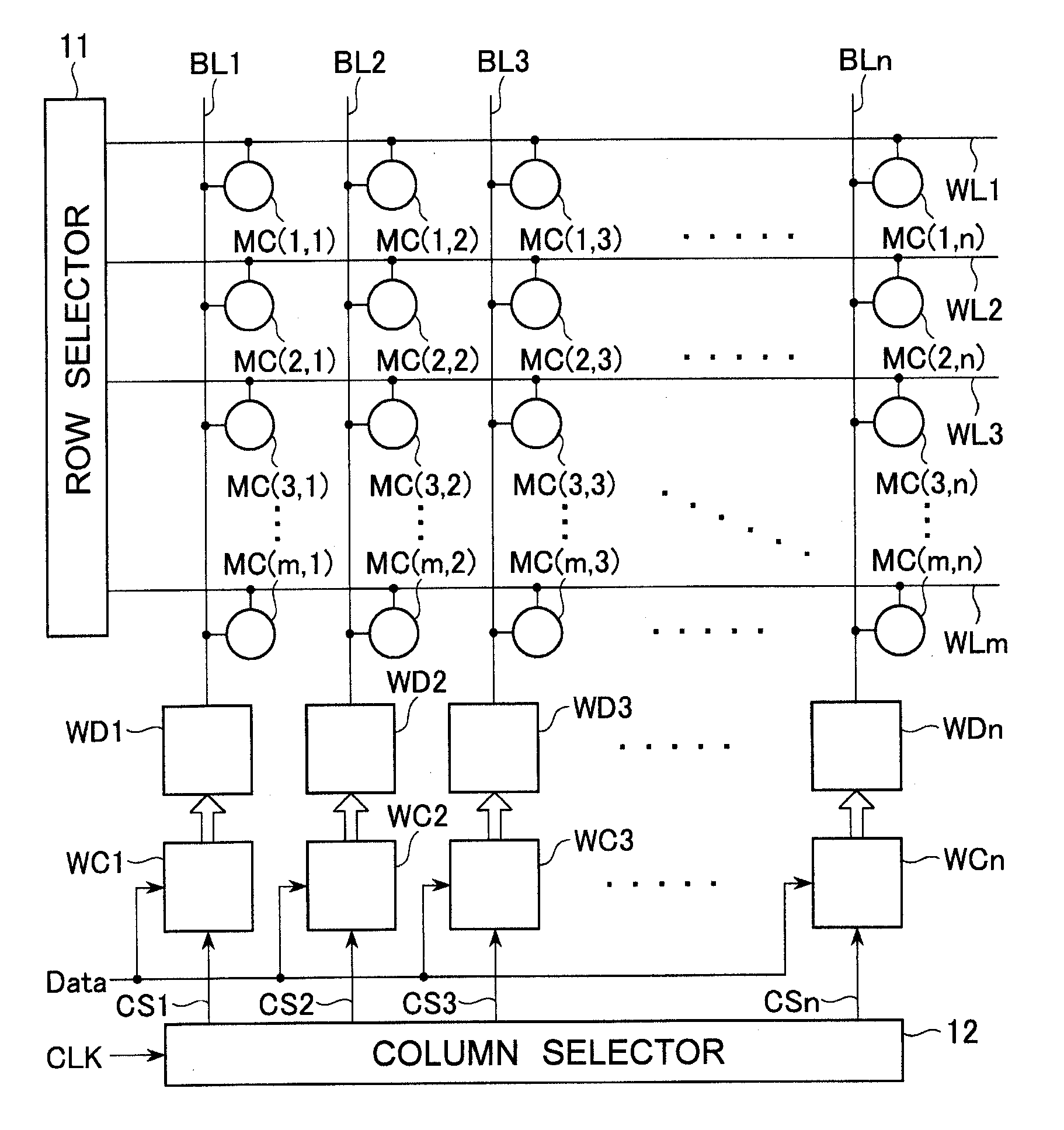
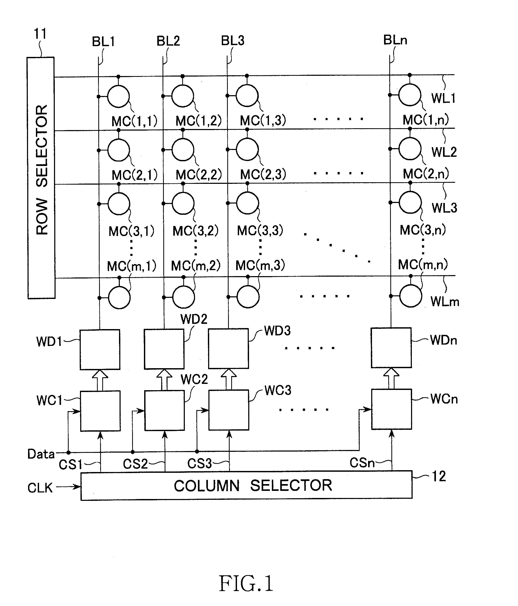
[0037]FIG. 1 is a circuit diagram for explaining the principle of a semiconductor memory device according to the present invention.

[0038]The semiconductor memory device shown in FIG. 1 is a matrix memory including word lines WL1 to WLm, bit lines BL1 to BLn intersecting the word lines WL1 to WLm, memory cells MC (1, 1) to MC (m, n) arranged at intersecting points between the word lines WL1 to WLm and the bit lines BL1 to BLn.

[0039]A row selector 11 selects one of the word lines WL1 to WLm and activates the selected word line WL. Write drivers WD1 to WDn are connected to the bit lines BL1 to BLn and supply electric current to the bit lines BL1 to BLn, respectively. Operations performed by the write drivers WD1 to WDn are controlled by write control circuits WC1 to WCn, respectively. As shown in FIG. 1, write data ‘Data’ is supplied to the write control circuits WC1 to W...


PUM


Abstract

A semiconductor memory device includes a plurality of word lines, a plurality of bit lines, a plurality of memory elements arranged at intersecting points between the word lines and the bit lines, respectively, a row selector selectively activating the word lines, a plurality of write drivers provided to correspond to the bit lines, and supplying a write current to the corresponding bit lines, respectively, a plurality of write control circuits controlling operations performed by the corresponding write drivers, respectively, and a column selector selecting the write control circuits. The column selector sequentially selects a predetermined write control circuit per one clock in a state of activating a predetermined word line, and the selected write control circuit activates one corresponding write driver over a period of one clock or more.

Description

TECHNICAL FIELD[0001]The present invention relates to a semiconductor memory device and a write control method thereof, and, more particularly to a semiconductor memory device having a write time difference according to a logical level of data to be written and a write control method for the semiconductor memory device.[0002]In personal computers or servers, hierarchically constructed various storage devices are used. A lower-hierarchical storage device is required to be low price and has a large capacity, while a higher-hierarchical one is required to be capable of high-speed access. As a lowest-hierarchical storage device, a magnetic storage such as a hard disk drive and a magnetic tape is generally used. The magnetic storage is nonvolatile and capable of saving a considerably large amount of data at a lower price as compared to a semiconductor memory device or the like. However, the magnetic storage is slow in access speed, and does not have random accessibility in many cases. Th...

Claims


Application Information

Patent Timeline
IPC IPC(8): G11C11/00
CPCG11C13/0004G11C13/02G11C13/0069
Inventor KATAGIRI, SATOSHI
Owner LONGITUDE LICENSING LTD
Why Eureka
Try Eureka