Two-dimensional Planar photonic crystal superprism device and method of manufacturing the same

a photonic crystal and superprism technology, applied in the field of two-dimensional planar photonic crystal superprism devices and a manufacturing method, can solve the problems of time taken to manufacture a photonic crystal device and difficulty in mass production, so as to save time, simplify a process, and reduce production costs

Inactive Publication Date: 2008-05-15
ELECTRONICS & TELECOMM RES INST
View PDF6 Cites 12 Cited by
  • Summary
  • Abstract
  • Description
  • Claims
  • Application Information

AI Technical Summary

Benefits of technology

[0008]The present invention is directed to a two-dimensional planar photonic crystal superprism device and a method of manufacturing the same that save time by simplifying a p

Problems solved by technology

However, according to such methods, the process is complex, and the number of process steps increase, thus creating a problem of inefficiency in that much time is taken

Method used


Image

  • Two-dimensional Planar photonic crystal superprism device and method of manufacturing the same
  • Two-dimensional Planar photonic crystal superprism device and method of manufacturing the same
  • Two-dimensional Planar photonic crystal superprism device and method of manufacturing the same

Examples


Embodiment Construction

[0028]Hereinafter, exemplary embodiments of the present invention will be described in detail. However, the present invention is not limited to the embodiments disclosed below, but can be implemented in various forms. Therefore, the following embodiments are described in order for this disclosure to be complete and enabling to those of ordinary skill in the art.

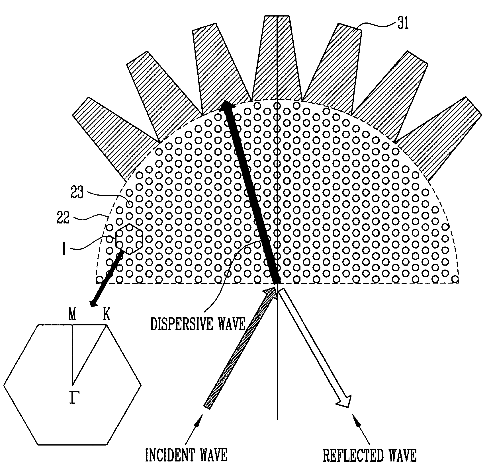
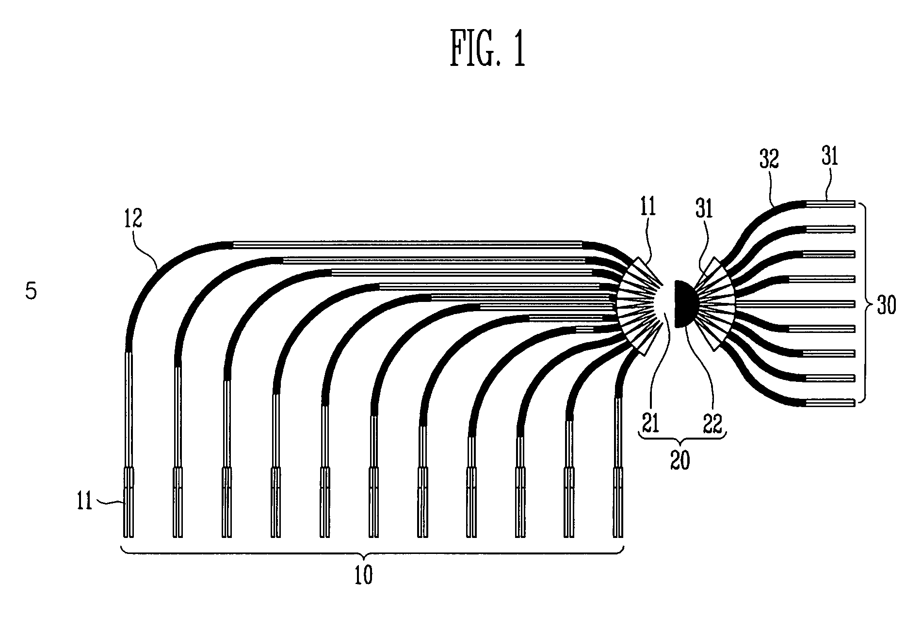
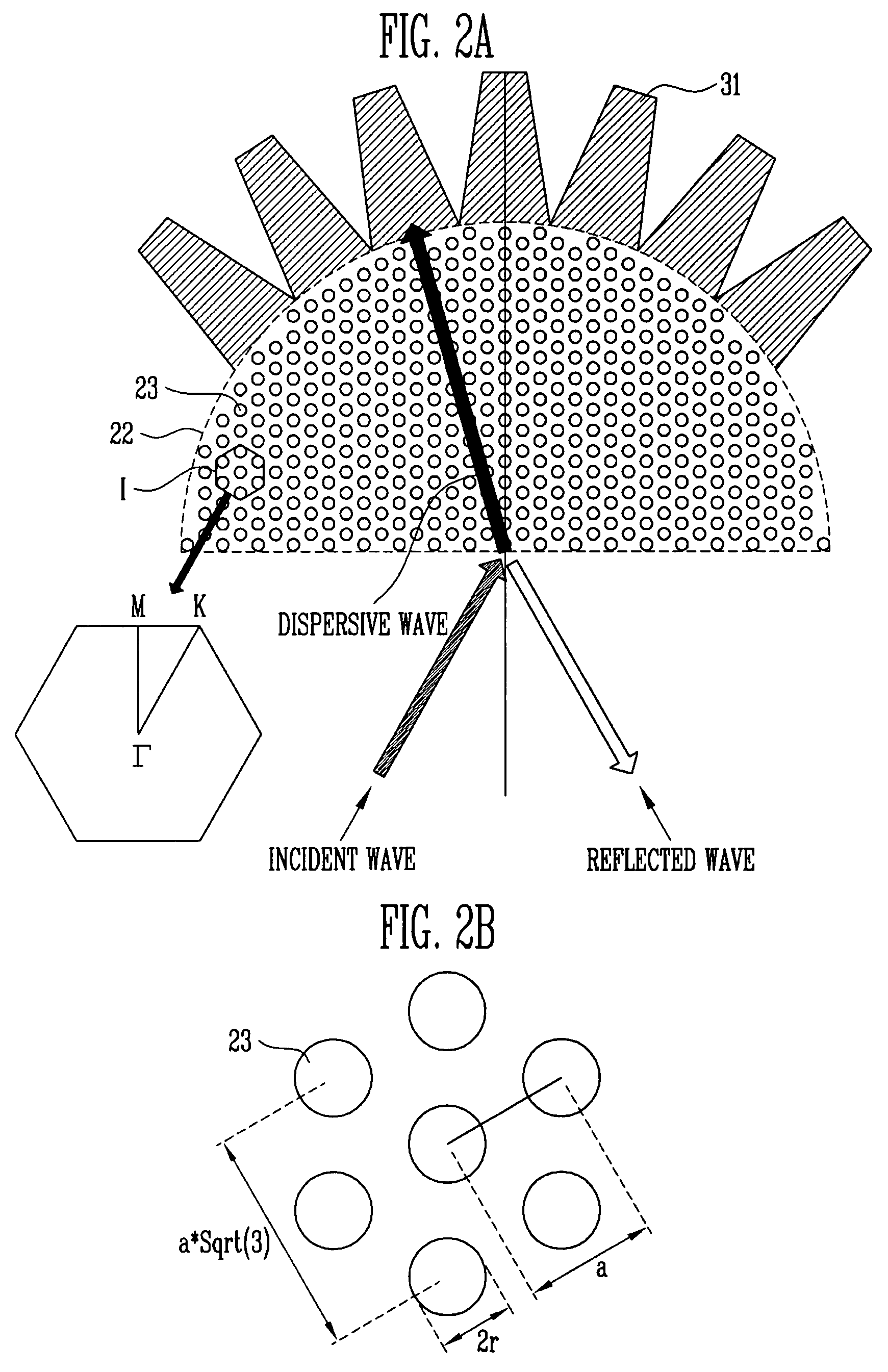
[0029]FIG. 1 is a schematic plan view showing the entire structure of a two-dimensional planar photonic crystal superprism device including input and output waveguides according to an exemplary embodiment of the present invention. Referring to FIG. 1, a two-dimensional planar photonic crystal superprism device 1 comprises single-mode input waveguides 10, a superprism 20, and single-mode output waveguides 30. In the two-dimensional planar photonic crystal superprism device 1, light waves are focused into a core layer and propagate in the horizontal direction by a two-dimensional photonic band gap (PBG) structure and in the ver...


PUM


Abstract

Provided are a two-dimensional planar photonic crystal superprism device and a method of manufacturing the same, in which a manufacturing process is simplified using a nanoimprint lithography technique, and thus price-reduction and mass production are facilitated. The two-dimensional planar photonic crystal superprism device includes: a single-mode input waveguide comprising a straight waveguide having a taper structure and a bending waveguide; a superprism formed on an output end side of the single-mode input waveguide and comprising a slab and a photonic crystal superprism; and a single-mode output waveguide comprising a straight waveguide having a taper structure and a bending waveguide, and formed adjacent to the photonic crystal superprism. Using the two-dimensional planar photonic crystal superprism device, it is possible to facilitate manufacturing of nano-photonic integrated circuits, photonic crystal integrated circuits and nano-photonic systems. In addition, a wavelength-selectable photonic crystal superprism device using high dispersion of photonic crystal, which is several hundred times the dispersion of conventional glass prism, can be manufactured using thermal/hot and ultraviolet nanoimprint lithography techniques corresponding to nano-manufacturing technology.

Description

CROSS-REFERENCE TO RELATED APPLICATION[0001]This application claims priority to and the benefit of Korean Patent Application Nos. 2006-110728, filed Nov. 9, 2006, and 2007-54852, filed Jun. 5, 2007, the disclosures of which are incorporated herein by reference in their entirety.BACKGROUND[0002]1. Field of the Invention[0003]The present invention relates to a two-dimensional planar photonic crystal superprism device and a method of manufacturing the same, and more particularly, to a two-dimensional planar photonic crystal superprism device and a method of manufacturing the same using a thermal / hot and ultraviolet (UV) imprint lithography technique that is nano-manufacturing technology. In other words, the present invention relates to a method of manufacturing a two-dimensional planar photonic crystal device used as a medium for transferring light using a polymer and a silicon-on-insulator (SOI) material, and more particularly, to a two-dimensional planar photonic crystal device, i.e....

Claims


Application Information

Patent Timeline
IPC IPC(8): G02B6/34G03F1/08
CPCB82Y20/00G02B6/1225G02B6/1221
Inventor CHOI, CHOON GIHAN, YOUNG TAKKIM, JIN TAELEE, WOO JIN
Owner ELECTRONICS & TELECOMM RES INST
Why Eureka
Try Eureka