Light emission device and display device

Inactive Publication Date: 2008-05-22
SAMSUNG SDI CO LTD
View PDF4 Cites 9 Cited by
  • Summary
  • Abstract
  • Description
  • Claims
  • Application Information

AI Technical Summary

Benefits of technology

[0010]Aspects of embodiments of the present invention are directed to a light emission device that includes front and rear substrates and is capable of quickly increasing electron emission efficiency and / or reducing a temperature difference between the front and rear substrates in an initial driving period of the light emission device and / or when the light emission device is driven under a low temperature environment. Other aspects of embodiments of the present invention are directed to a display device using the light emission device as a light source.

Problems solved by technology

In an initial driving state of the light emission device or when the light emission device is driven under a low temperature environment, electron emission cannot be sufficiently realized due to the rear substrate being in a low temperature state.
That is, it takes a relatively long time to increase an emission amount of electrons to a proper level with a certain (or predetermined) driving voltage to thus stabilize the electron emission property.
Furthermore, when the light emission device is being driven, there may be a temperature difference between the front and rear substrates.
This temperature difference may cause cracks to be generated on and / or in the substrates, thereby deteriorating lifespan and reliability of the light emission device.
The temperature difference also adversely affects the spacers arranged between the front and rear substrates by varying a surface potential of the spacers, thereby deteriorating an electron beam path around the spacers.

Method used


Image

  • Light emission device and display device
  • Light emission device and display device
  • Light emission device and display device

Examples


second embodiment

[0063]FIG. 5 is a sectional view of a surface heat generation unit according to the present invention. Referring to FIG. 5, when the luminance variation occurs along a length (an x-axis in FIG. 5) of one of the driving electrodes, the PTC resistive layer 581 is designed having a thickness that varies along the length of the driving electrode; i.e., the PTC resistive layer 581 is thicker at a portion where the luminance is low.

third embodiment

[0064]FIG. 6 is a sectional view of a surface heat generation unit according to the present invention. Referring to FIG. 6, when the light emission luminance is gradually lowered toward the peripheral portion from the central portion of the light emission surface, a thickness of the PTC resistive layer 582 increases gradually from the central portion toward the peripheral portion.

fourth embodiment

[0065]FIG. 7 is a sectional view of a surface heat generation unit according to the present invention. Referring to FIG. 7, when the light emission luminance is gradually lowered toward the central portion from the peripheral portion of the light emission surface, a thickness of the PTC resistive layer 583 increases gradually from the peripheral portion toward the central portion.

[0066]As described above, the PTC resistive layers 581, 582, 583 are formed to be thicker at a portion where the light emission luminance is low and thus the electron emission efficiency at the portion where the light emission luminance is low increases during the operation of the light emission panel 20. As a result, a luminance irregularity of the light emission surface can be reduced.

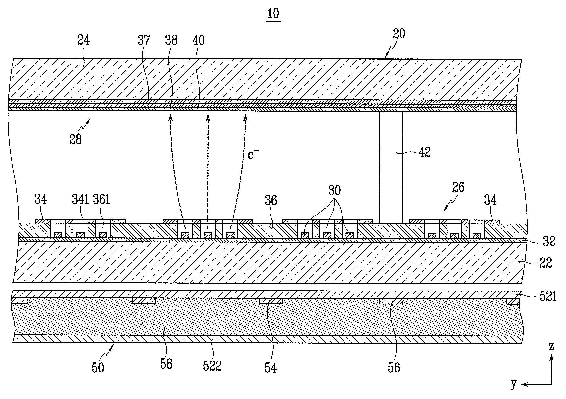
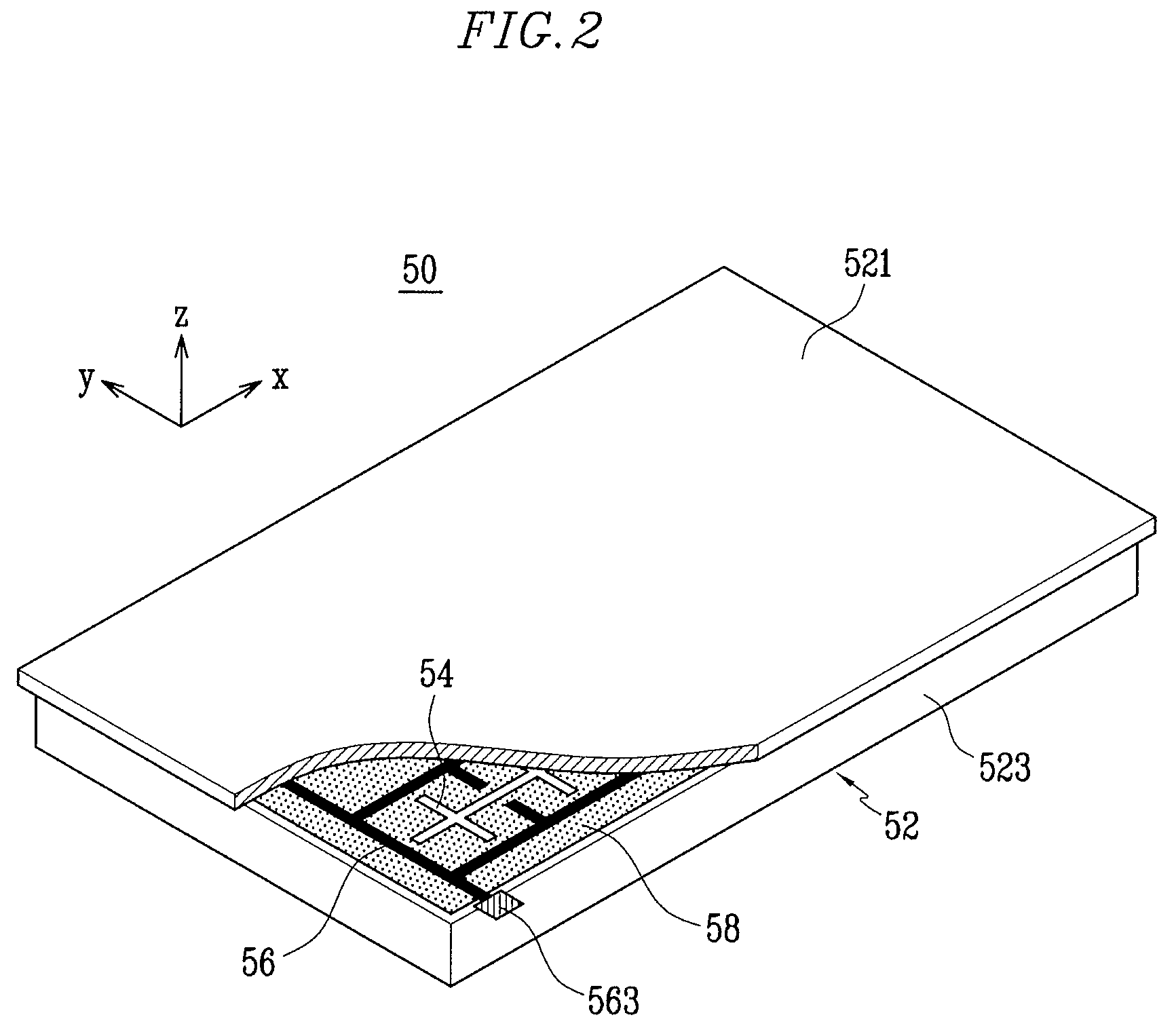
[0067]The light emission device 10 may be used as a display device (by itself) by being provided with red, green, and blue phosphor layers or as a light source for providing white light to a passive type display panel.

[0068]...


PUM


Abstract

A light emission device and a display device having the light emission device are provided. The light emission device includes first and second substrates that are arranged to face each other, an electron emission unit that is located on a first surface of the first substrate facing the second substrate and has electron emission regions and driving electrodes, a light emission unit that is located on a surface of the second substrate and has an anode electrode and one or more phosphor layers, and a surface heat generation unit that is located on a second surface (or outer surface) of the first substrate facing away from the second substrate to control a temperature of the first substrate using a resistive layer having a positive temperature coefficient (PTC) property.

Description

CROSS-REFERENCE TO RELATED APPLICATION[0001]This application claims priority to and the benefit of Korean Patent Application No. 10-2006-0114615, filed on Nov. 20, 2006, in the Korean Intellectual Property Office, the entire content of which is incorporated herein by reference.BACKGROUND OF THE INVENTION[0002]1. Field of the Invention[0003]The present invention relates to a light emission device that is designed to control a temperature of a rear substrate on which electron emission regions are located. The present invention further relates to a display device using the light emission device as a light source.[0004]2. Description of Related Art[0005]Devices that can emit light to an external side can be referred to as light emission devices. One type of light emission devices includes a rear substrate on which electron emission regions and driving electrodes are formed, and a front substrate on which an anode electrode and a phosphor layer are formed. This light emission device emit...

Claims


Application Information

Patent Timeline
IPC IPC(8): H01J7/24
CPCG02F2001/133625H01J29/96H01J2329/86H01J61/305H01J63/02H01J31/127G02F1/133625H01J1/30H01J1/62H01J7/24H01J7/34
Inventor PARK, SANG-HUN
Owner SAMSUNG SDI CO LTD
Why Eureka
Try Eureka