
Adjustable anode assembly for a substrate wet processing apparatus

a technology of wet processing apparatus and anode assembly, which is applied in the direction of machining electrodes, manufacturing tools, electrical-based machining electrodes, etc., can solve the problems of uncontrollable or varied electrical field density distribution within the chemical, device characteristics across the wafer that are undesired or cannot be selectively varied

Inactive Publication Date: 2008-05-29
TAIWAN SEMICON MFG CO LTD
View PDF9 Cites 14 Cited by
  • Summary
  • Abstract
  • Description
  • Claims
  • Application Information

AI Technical Summary

Benefits of technology

The patent describes an apparatus for manufacturing integrated circuits using a wafer or substrate processing apparatus. The apparatus includes a cell with an anode having an adjustable shape, which can be adjusted to change the space between the wafer or substrate and the anode. This allows for selective adjustment of the space across the wafer or substrate in height. The method involves placing the wafer or substrate in the cell, adjusting the shape of the anode, and operating the apparatus to process the wafer, thereby forming the integrated circuit. The technical effect of this invention is to provide a more precise and flexible method for manufacturing integrated circuits, allowing for better control over the processing conditions and resulting in higher quality circuits.

Problems solved by technology

One drawback of these wet processing apparatuses is that the height of the three-dimensional space between the anode and the wafer is the same across the entire wafer, consequently, the electrical field density distribution within the chemical cannot be controlled or varied.
As semiconductor wafers increase in size and minimum device feature size decreases, the inability to control the electrical field density distribution within the chemical in the space will lead to device characteristics across the wafer that are undesired or which can not be selectively varied.

Method used


Image

  • Adjustable anode assembly for a substrate wet processing apparatus
  • Adjustable anode assembly for a substrate wet processing apparatus
  • Adjustable anode assembly for a substrate wet processing apparatus

Examples


Embodiment Construction

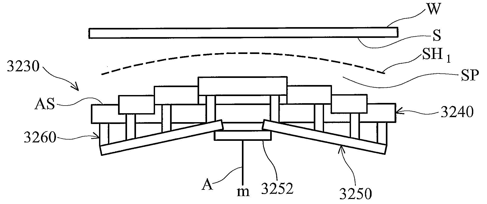
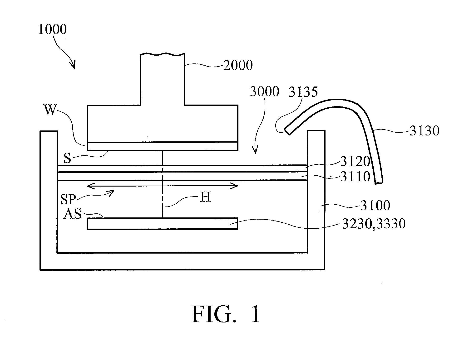
[0032]Disclosed herein is an adjustable anode assembly for an apparatus of the type which may be used in the wet processing of semiconductor wafers and other wafers and substrates. The adjustable anode assembly may be used in any wet processing or like apparatus that uses an anode including, for example but not limited to, electrochemical plating (ECP) apparatuses and an electrochemical mechanical polishing (ECMP) apparatuses. For ease in describing the adjustable anode, the same will be described with reference to an ECP apparatus, an embodiment of which is shown FIG. 1. The ECP apparatus, denote by numeral 1000 generally comprises a cell assembly 3000 and a carrier head assembly 2000 for holding a semiconductor wafer W or any other wafer or substrate to be wet processed in the cell assembly 3000 and for delivering DC power to the wafer W during plating and deplating.

[0033]The cell assembly 3000 forms a container or electroplating cell 3100 for confining an electrolyte plating solu...


PUM

PropertyMeasurementUnit
diameteraaaaaaaaaa
diameteraaaaaaaaaa
diameteraaaaaaaaaa

Abstract

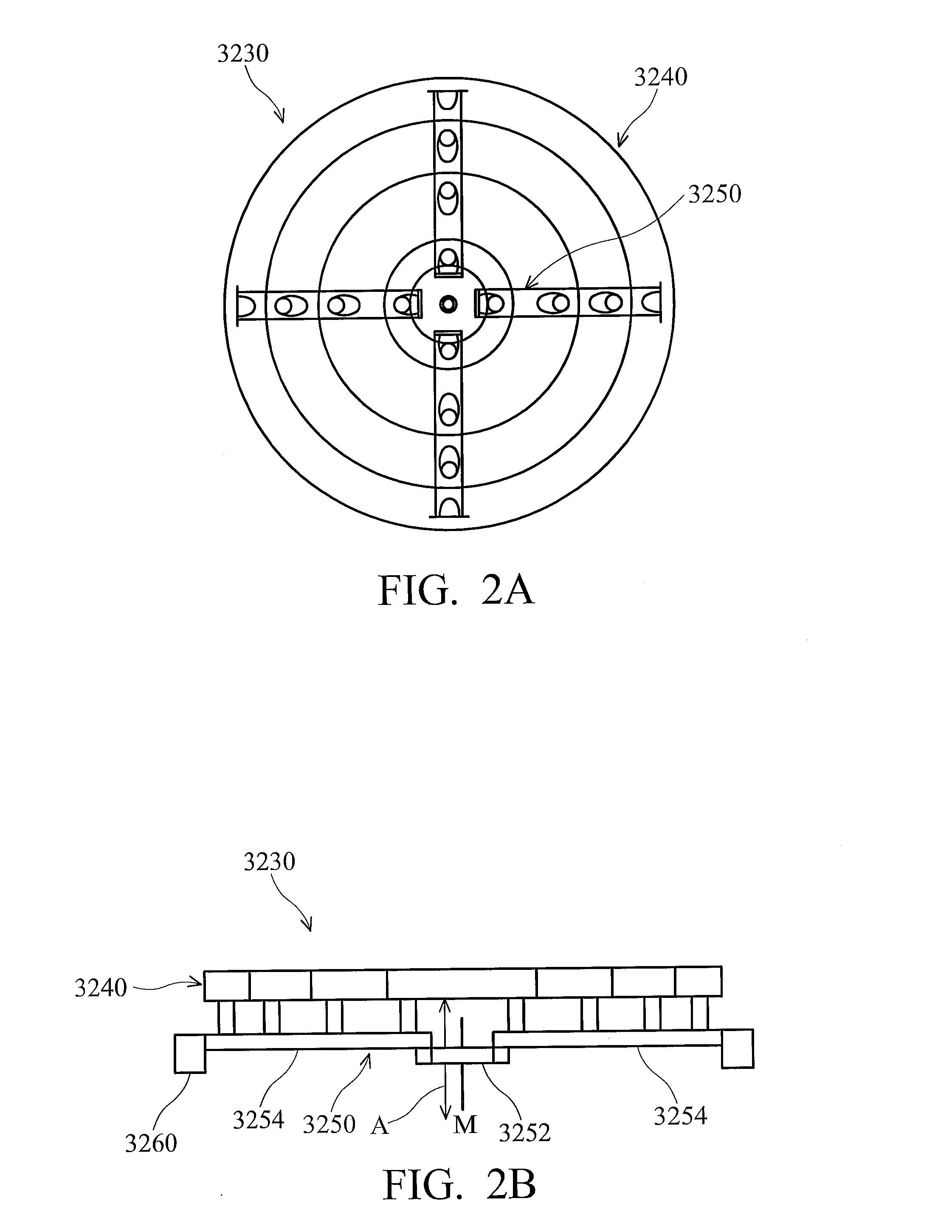
An adjustable anode assembly for a wet processing apparatus to allow selective tuning of the electrical field density distribution within a wet process chemical of the apparatus, which in turn allows the process specification or specifications to be selectively varied across the process surface of a wafer when processed by the apparatus. The adjustable anode assembly includes an anode which may be divided into several plates, at least one of which is capable of being moved from a first plane to at least a second plane.

Description

FIELD OF THE INVENTION[0001]The present invention relates to semiconductor fabrication. In particular, the present invention relates to an apparatus and method for providing an anode-to-wafer gap that varies in height or thickness across the surface of a wafer to be wet processed in a wet processing apparatus.BACKGROUND OF THE INVENTION[0002]Many wet processes are performed in semiconductor fabrication. These processes may include electrochemical plating (ECP), electrochemical mechanical polishing (ECMP), spin-coating, cleaning and etching, to name some examples. Hence, many apparatuses have been designed and are currently available for wet processing wafers and other substrates.[0003]A typical wet processing apparatus may include a process cell for confining a process chemical and a carrier head that holds a wafer within the cell so that it may be treated by the chemical contained in or introduced into the cell. In wet processing apparatuses, (e.g., ECP and ECMP apparatuses), the c...

Claims


Application Information

Patent Timeline
Patent Type & Authority Applications(United States)
IPC IPC(8): C25D5/04C25D17/10C25D17/00
CPCC25D17/12C25D7/12C25D17/001C25D7/123
Inventor HSIAO, YI-LIYU, CHEN-HUAWANG, JEANSHEU, LAWRANCE
Owner TAIWAN SEMICON MFG CO LTD
Learn More