Nonvolatile memory cell, array thereof, fabrication methods thereof and device comprising the same

a nonvolatile memory and array technology, applied in the direction of semiconductor devices, electrical devices, nanotechnology, etc., can solve the problems of large current leakage, nonvolatile memory may function abnormally, and current leakage may be significantly increased, so as to reduce current leakage

Active Publication Date: 2008-05-29
SAMSUNG DISPLAY CO LTD
View PDF12 Cites 2 Cited by
  • Summary
  • Abstract
  • Description
  • Claims
  • Application Information

AI Technical Summary

Problems solved by technology

Thus, surfaces of the polysilicon layers may be rough and non-uniform, which may result in a large current leakage being generated.
In other words, a current leakage may be significantly increased due to the non-uniformity and roughness of the surfaces of the polysilicon layer.
Therefore, such a nonvolatile memory may function abnormally during storing / erasing operations

Method used


Image

  • Nonvolatile memory cell, array thereof, fabrication methods thereof and device comprising the same
  • Nonvolatile memory cell, array thereof, fabrication methods thereof and device comprising the same
  • Nonvolatile memory cell, array thereof, fabrication methods thereof and device comprising the same

Examples


Embodiment Construction

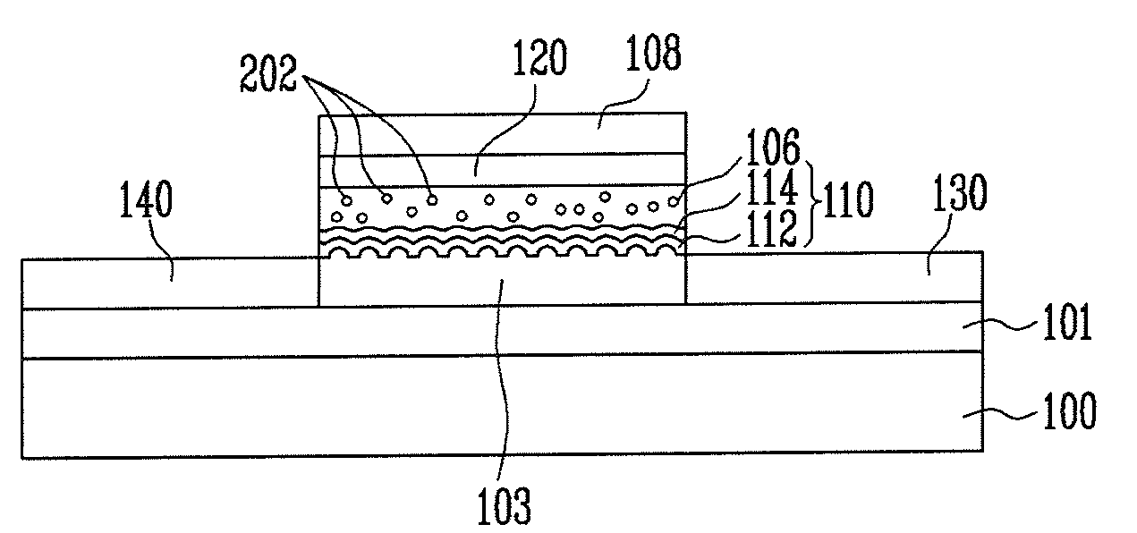
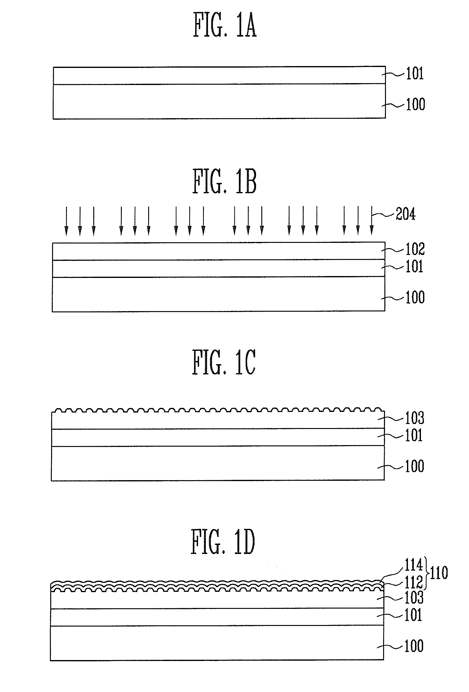
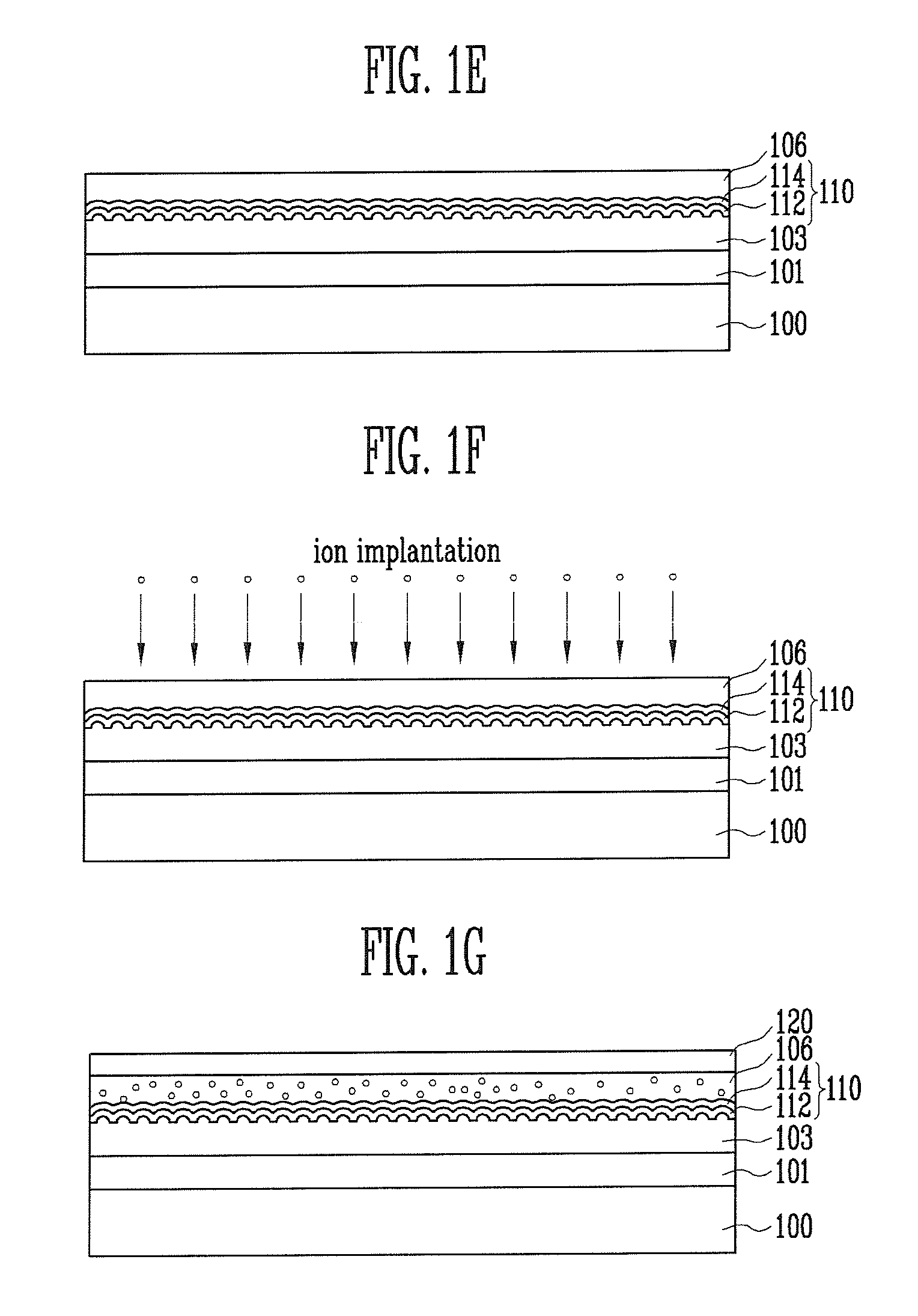
[0025]Reference will now be made in detail to the various embodiments of the present invention, examples of which are illustrated in the accompanying drawings, wherein like reference numerals refer to the like elements throughout. The exemplary embodiments are described below in order to explain the present invention by referring to the figures.

[0026]In the figures, the dimensions of the various layers and regions may be exaggerated for clarity. It will also be understood that when a layer or element is referred to as being “on” another layer or substrate, it can be directly on the other layer or substrate, or intervening layers may also be present. Further, it will be understood that when a layer is referred to as being “under” another layer, it can be directly under, or one or more intervening layers may also be present.

[0027]In addition, it will also be understood that when a layer is referred to as being “between” two layers, it can be the only layer between the two layers, or o...


PUM

PropertyMeasurementUnit
temperatureaaaaaaaaaa
ion acceleration energyaaaaaaaaaa

Abstract

A nonvolatile memory cell is capable of reducing an excessive current leakage due to a rough surface of a polysilicon and of performing even at a low temperature process by forming the first oxide film including a silicon oxynitride (SiOxNy) layer using nitrous oxide plasma and by forming a plurality of silicon nanocrystals in a nitride film by implanting a silicon nanocrystal on the nitride film by an ion implantation method, and a fabricating method thereof and a memory apparatus including the nonvolatile memory cell.

Description

CROSS-REFERENCE TO RELATED APPLICATIONS[0001]This application claims the benefit of Korean Application No. 2006-117153, filed Nov. 24, 2006, in the Korean Intellectual Property Office, the disclosure of which is incorporated herein by reference.BACKGROUND OF THE INVENTION[0002]1. Field of the Invention[0003]Aspects of the present invention relate to a nonvolatile memory cell and a fabrication method thereof.[0004]2. Description of the Related Art[0005]Generally, nonvolatile memory devices may be classified as floating-gate memory devices and charge-trapping memory devices. Floating-gate memory devices are devices that maintain a charge by using a potential well. Charge-trapping memory devices are devices that trap charges in a trap region inside a nitride film, or in a trap region present in an interface between a nitride film and an insulator.[0006]A representative form of a charge-trapping memory device is a Silicon-Oxide-Nitride-Oxide-Silicon (SONOS) configuration. Typically, the...

Claims


Application Information

Patent Timeline
Patent Type & Authority Applications(United States)
IPC IPC(8): H01L29/06H01L21/336
CPCB82Y10/00H01L21/28273H01L21/84H01L27/115H01L27/11521H01L27/11524H01L29/7881H01L29/04H01L29/1037H01L29/42332H01L29/513H01L29/66825H01L27/12Y10S977/773Y10S977/723Y10S977/721Y10S977/774Y10S977/72Y10S977/784Y10S977/785H01L29/40114H10B41/35H10B69/00H10B41/30H01L21/28202
Inventor CHOI, BYOUNG DEOGYI, JUN SINJUNG, SUNG WOOKHWANG, SUNG HYUNG
Owner SAMSUNG DISPLAY CO LTD
Why Eureka
Try Eureka