Circuit for discharging static electricity

a static electricity and circuit technology, applied in the field of circuits for discharging static electricity, can solve the problems of difficult realization of small sized and high-speed semiconductor devices, critical damage to circuit devices, etc., and achieve the effect of reducing the capacitance of pins and reducing the area of electrostatic discharge circuits

Active Publication Date: 2008-05-29
SK HYNIX INC
View PDF4 Cites 4 Cited by
  • Summary
  • Abstract
  • Description
  • Claims
  • Application Information

AI Technical Summary

Benefits of technology

[0015]The present invention provides a device for discharging static electricity, which decreases...

Problems solved by technology

When a high voltage ESD current is introduced to an internal circuit of a semiconductor device with a designed power voltage of lower than 5V, circ...

Method used


Image

  • Circuit for discharging static electricity
  • Circuit for discharging static electricity
  • Circuit for discharging static electricity

Examples


first embodiment

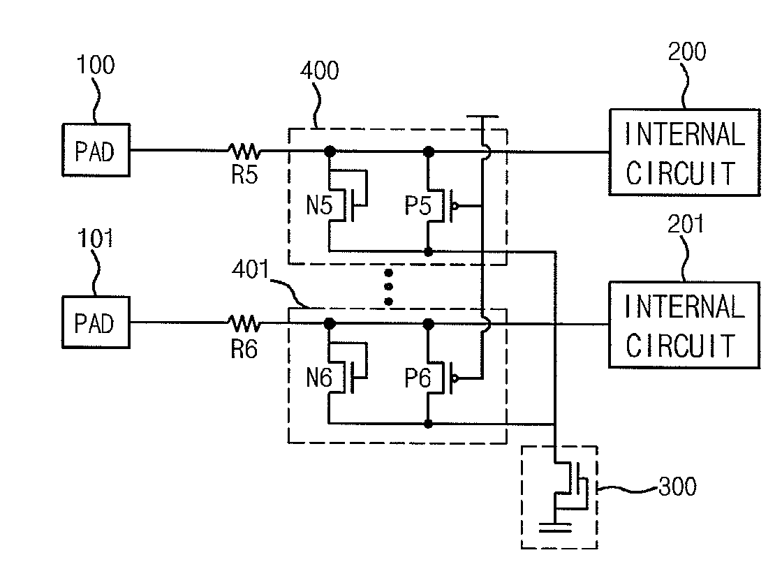
[0038]In an operation of FIG. 3, in a case of a test mode, PMOS transistors P5 and P6 are always turned on since the external power voltage (VDD) is not applied.

[0039]At this time, in a path through which charges accumulated in the ground of the semiconductor device flow to the respective input / output pads 100 and 101, for example, when a positive static electricity is generated, PMOS transistors P5 and P6 of the switching units 400 and 401 are turned on to form a path in which the charges flow out through the discharge unit 300. To the contrary, when a negative static electricity is generated, NMOS transistors N5 and N6 of the switching units 400 and 401 are turned on by NP diode operation to form a current path connected with the discharge unit 300 thereby protecting safely the internal circuits 100 and 101. As such, the discharge unit 300 is commonly used for protecting respective internal circuits 100 and 101.

[0040]Next, since the external power voltage is applied during normal ...

second embodiment

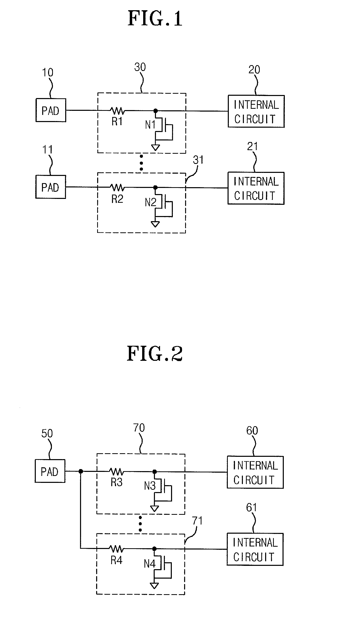
[0041]Meanwhile, FIG. 4 shows a case that respective internal circuits 600 and 601 are connected to the same input / output pad 500 and the internal circuits 600 share entire circuit for discharging static electricity.

[0042]More specifically, a switching unit 800 is connected between the internal circuit 600 and the input / output pad 500 and a discharge unit 700 is serially connected with the switching unit 800. Further, a switching unit 801 is connected between the internal circuit 601 and the input / output pad 500 and the discharge unit 700 is also serially connected with the switching unit 801. As a result, the discharge unit 700 is commonly connected to the plurality of the internal circuits 600 and 601 and thus be shared.

[0043]In addition, a resistor R7 is connected between the input / output pad 500 and the respective switching units 800 and 801 to be shared by the switching units 800 and 801.

[0044]Herein, the switching unit 800 is the same as that of the first embodiment. In other ...


PUM


Abstract

The present invention relates to a semiconductor circuit, and more particularly, to a circuit for discharging static electricity, which is connected between an internal circuit and an input/output pad to provide a charge device model (CDM) discharging path. The circuit includes a plurality of input/output pads; a plurality of switching units corresponding one-to-one to the input/output pads and turned on in a low voltage state; resistors connected between the input/output pads and the switching units so as to correspond one-to-one to the input/output pads and the switching units; and a CDM discharge unit shared in serial by the plurality of the switching units and providing a ground path.

Description

CROSS-REFERENCE TO RELATED APPLICATIONS[0001]The present application claims priority to Korean patent application number 10-2006-0061587 filed on Jun. 30, 2006, which is incorporated herein by reference in its entirety.BACKGROUND OF THE INVENTION[0002]The present invention relates to a semiconductor circuit, and more particularly, to a circuit for discharging static electricity, which is connected between an internal circuit and an input / output pad to provide a charge device model (CDM) discharging path.[0003]Generally, electrostatic discharge (ESD) is a rapid flow of electric current when two mutually insulated objects with significantly different potentials come into direct contact with each other and an electrostatic discharging circuit is formed between an internal circuit of a semiconductor chip and a pad to be connected with input / output pins for preventing destruction or degradation of a product due to static electricity when designing a semiconductor device.[0004]When a high...

Claims


Application Information

Patent Timeline
IPC IPC(8): H02H9/04
CPCH02H9/046H01L27/04
Inventor KIM, JANG HOO
Owner SK HYNIX INC
Why Eureka
Try Eureka