Semiconductor Device Manufactured Using Passivation of Crystal Domain Interfaces in Hybrid Orientation Technology

a crystal domain interface and semiconductor technology, applied in the field of semiconductor devices, can solve the problems of physical limits of feature size, slow device performance increase rate, and device characteristics may be degraded

Inactive Publication Date: 2008-06-05
TEXAS INSTR INC
View PDF9 Cites 3 Cited by
  • Summary
  • Abstract
  • Description
  • Claims
  • Application Information

AI Technical Summary

Benefits of technology

[0008]Another embodiment is a semiconductor device. The semiconductor device has a first substrate with a crystal orientation, and a second substrate with a different crystal orientation located over the first substrate. An interfacial region exists between the first and second substrates. A pa

Problems solved by technology

As the semiconductor industry continues to increase performance of integrated circuit devices in accordance with Moore's Law, physical limits of feature size are presenting new challenges to further improvement.
Without new strategies, such challenges threaten to slow the rate of increase in device performance.
While some transistors formed on a HOT substrate may operate faster than they otherwise would, some device characteristics may be degraded.
Moreover, body contact from the transistors to the handle wafer may be non-ohmic.
These effects may result in increase power dissipation and inadequate grounding of the integrated circuit.

Method used


Image

  • Semiconductor Device Manufactured Using Passivation of Crystal Domain Interfaces in Hybrid Orientation Technology
  • Semiconductor Device Manufactured Using Passivation of Crystal Domain Interfaces in Hybrid Orientation Technology
  • Semiconductor Device Manufactured Using Passivation of Crystal Domain Interfaces in Hybrid Orientation Technology

Examples


Embodiment Construction

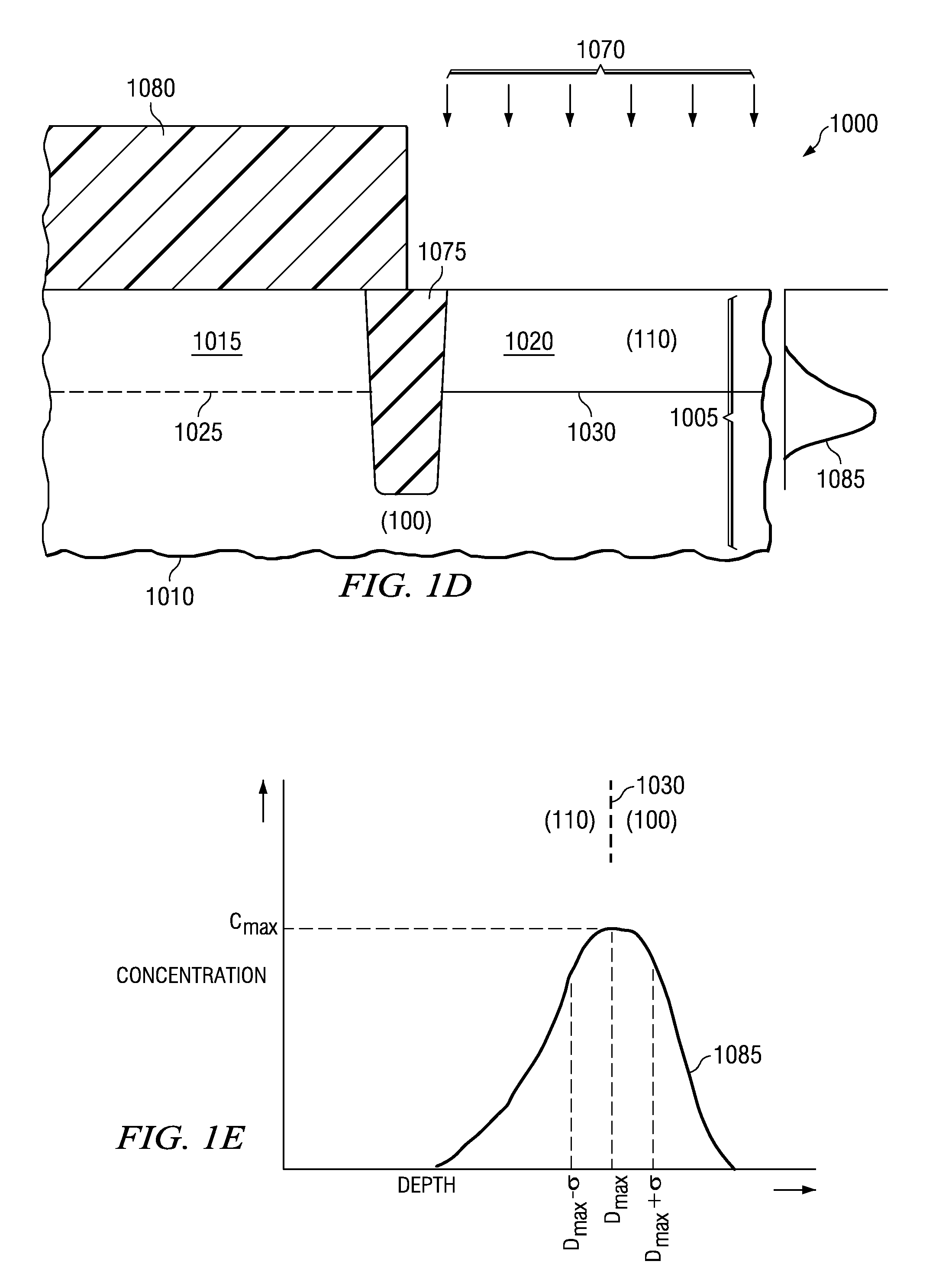
[0015]The invention recognizes that undesirable transistor characteristics associated with an interface between different crystal orientations of a hybrid-crystal orientation technology (HOT) substrate may be reduced by passivating unterminated bonds associated with lattice mismatch at the interface. Passivation may be accomplished, e.g., by implanting a passivating dopant that bonds to the unterminated bonds.

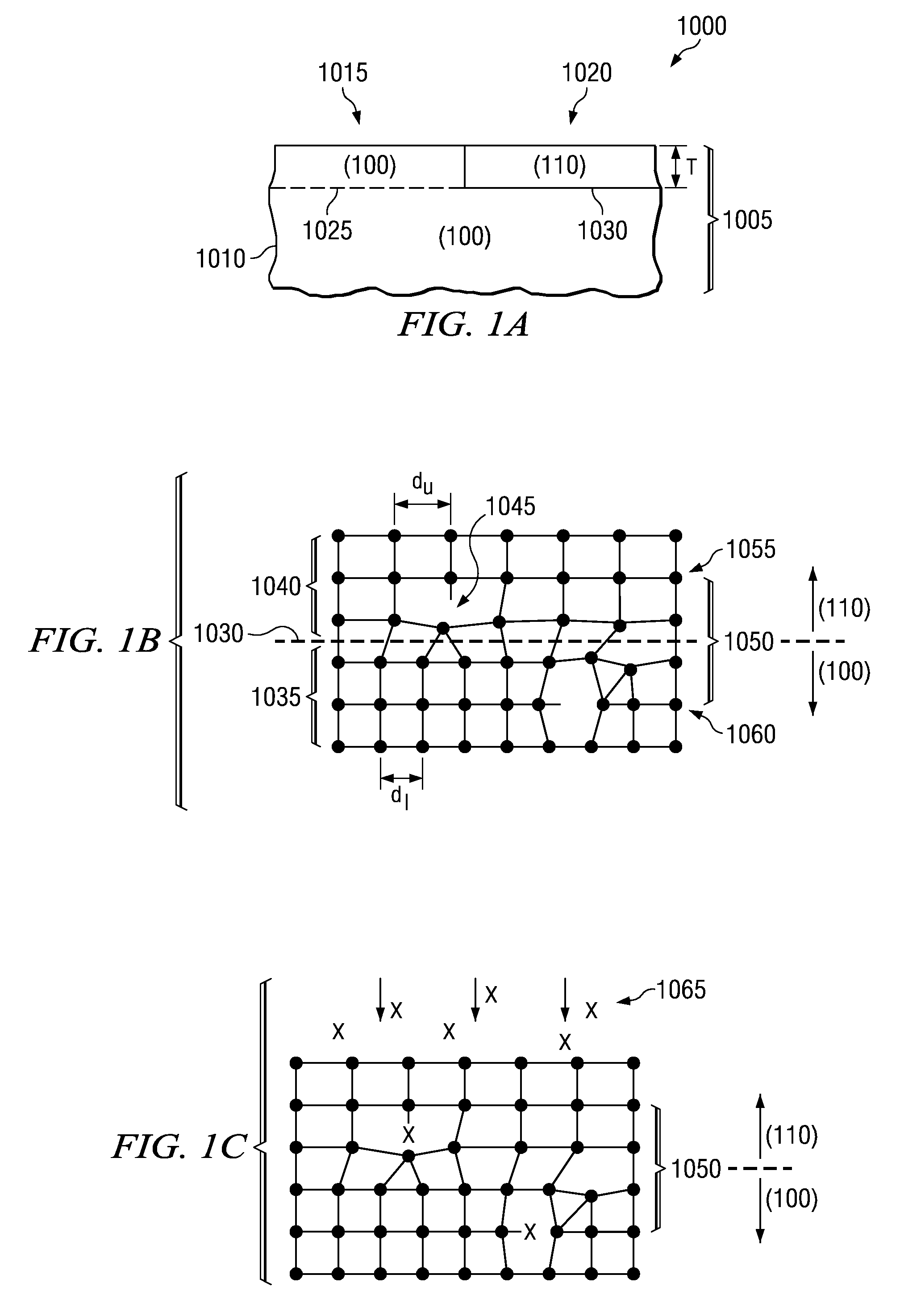
[0016]FIG. 1A illustrates a semiconductor device 1000 formed according to the invention. It is initially noted that, unless otherwise discussed, conventional processes and materials may be used to fabricate certain portions of the devices regarding the various embodiments discussed herein. The semiconductor device 1000 includes a HOT substrate 1005 that further includes a bulk portion 1010, an epitaxial portion 1015 and a hybrid portion 1020 with a thickness T. The epitaxial portion 1015 is substantially an extension of the lattice of the bulk portion 1010. Thus, the illustrate...


PUM


Abstract

The invention provides, in one aspect, a method of forming a semiconductor device including providing a semiconductor substrate that comprises a first portion having a crystal orientation and a second portion located over the first portion and having a different crystal orientation. An interfacial region is located between the first portion and second portion. A passivating dopant is implanted into the interfacial region to passivate unterminated bonds within the interfacial region.

Description

TECHNICAL FIELD OF THE INVENTION[0001]The invention is directed, in general, to semiconductor devices and, more specifically, to semiconductor devices fabricated using passivation of unterminated bonds in an interfacial region associated with regions of different crystal orientation.BACKGROUND OF THE INVENTION[0002]As the semiconductor industry continues to increase performance of integrated circuit devices in accordance with Moore's Law, physical limits of feature size are presenting new challenges to further improvement. For example, transistor gate lengths are approaching a value below which quantum effects cannot be neglected. Without new strategies, such challenges threaten to slow the rate of increase in device performance.[0003]One such strategy involves increasing the mobility of minority charge carriers in a transistor so that the switching speed of the transistor may be increased without reducing the channel length of the transistor. A promising emerging technology dubbed...

Claims


Application Information

Patent Timeline
IPC IPC(8): H01L29/04H01L21/8238
CPCH01L21/823807H01L29/7833H01L29/045H01L27/092
Inventor PINTO, ANGELOCHIDAMBARAM, P.R.CHAKRAVARTHI, SRINIVASANWISE, RICK L.
Owner TEXAS INSTR INC
Why Eureka
Try Eureka