Organic inverter including surface-treated layer and method of manufacturing the same
- Summary
- Abstract
- Description
- Claims
- Application Information
AI Technical Summary
Benefits of technology
Problems solved by technology
Method used
Image

Examples
Embodiment Construction
[0021]The present invention will now be described more fully hereinafter with reference to the accompanying drawings, in which exemplary embodiments of the present invention are shown.
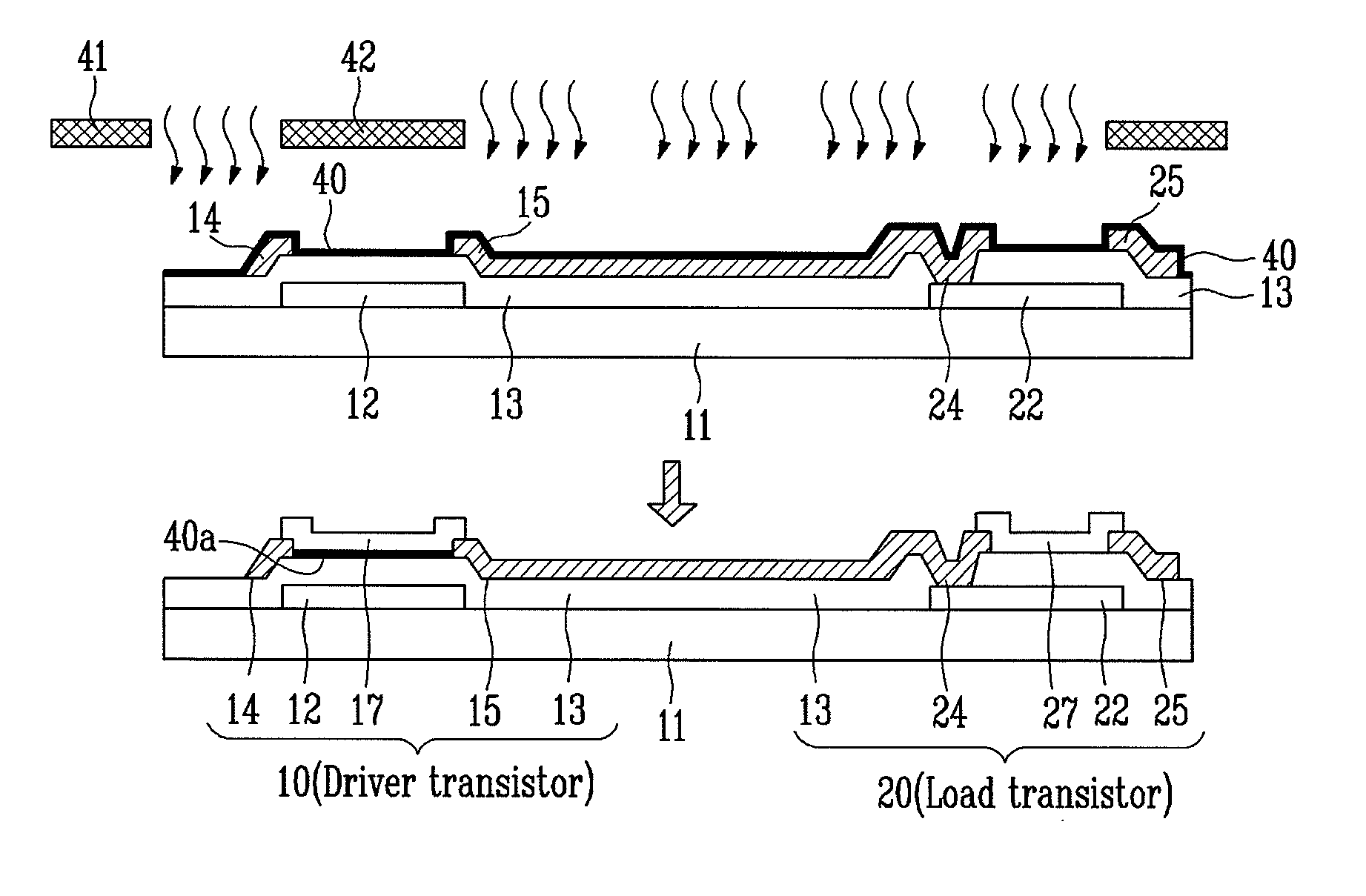
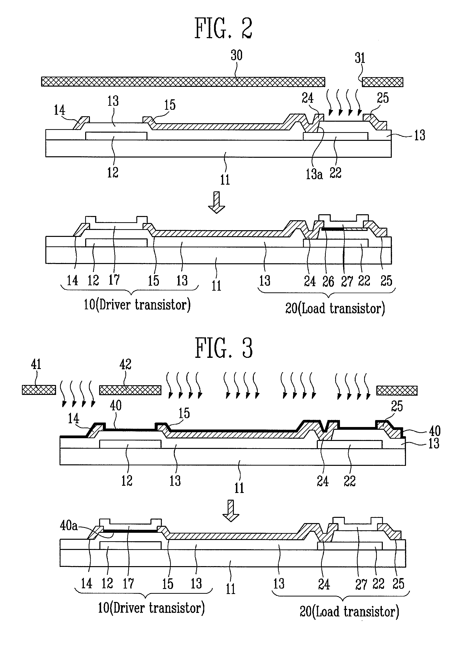
[0022]FIGS. 2 and 4 are cross-sectional views partially illustrating a manufacturing process of an organic inverter according to first to third exemplary embodiments of the present invention.
[0023]Referring to FIG. 2 illustrating a first exemplary embodiment, to manufacture an organic inverter including a driver transistor 10 and a load transistor 20 according to the present invention, a substrate 11 is first prepared. A pair of gate electrodes 12 and 22 are then formed on the prepared substrate 11. After forming the gate electrodes 12 and 22, a gate insulating layer 13 is formed on the gate electrodes 12 and 22. Then, source and drain electrodes 14 and 15 of the driver transistor 10, and source and drain electrodes 24 and 25 of the load transistor 20 are formed on the gate insulating layer 13. Here, t...
PUM
 Abstract
Description
Claims
Application Information
 - R&D Engineer
- R&D Manager
- IP Professional
- Industry Leading Data Capabilities
- Powerful AI technology
- Patent DNA Extraction
Browse by: Latest US Patents, China's latest patents, Technical Efficacy Thesaurus, Application Domain, Technology Topic.
© 2024 PatSnap. All rights reserved.Legal|Privacy policy|Modern Slavery Act Transparency Statement|Sitemap