Thin film transistor and fabrication method thereof

a technology of thin film transistors and fabrication methods, applied in the direction of basic electric elements, electrical equipment, semiconductor devices, etc., can solve the problems of crystal grain uniformity decrease, low mobility, and difficulty in driving the pixel portion

Active Publication Date: 2008-06-19
SAMSUNG DISPLAY CO LTD
View PDF3 Cites 18 Cited by
  • Summary
  • Abstract
  • Description
  • Claims
  • Application Information

AI Technical Summary

Problems solved by technology

However, in this case, the electron mobility is so low that it is difficult to drive the pixel portion.
However, since the annealed polycrystalline silicon layer has a number of defects in a crystal grain, a lot of leakage current is generated and the crystal grain decreases in uniformity, making it difficult to display an image with uniform brightness.
Further, not only does it take a lot of time to perform the annealing, but also an additional process such as the laser annealing causes a fabricating process to become complicated.
Therefore, the time taken to move a stage is lengthened, thereby increasing a processing time.

Method used


Image

  • Thin film transistor and fabrication method thereof
  • Thin film transistor and fabrication method thereof
  • Thin film transistor and fabrication method thereof

Examples


Embodiment Construction

[0021]a Reference will now be made in detail to the present embodiments of the present invention, examples of which are illustrated in the accompanying drawings, wherein like reference numerals refer to the like elements throughout. The embodiments are described below in order to explain the present invention by referring to the figures.

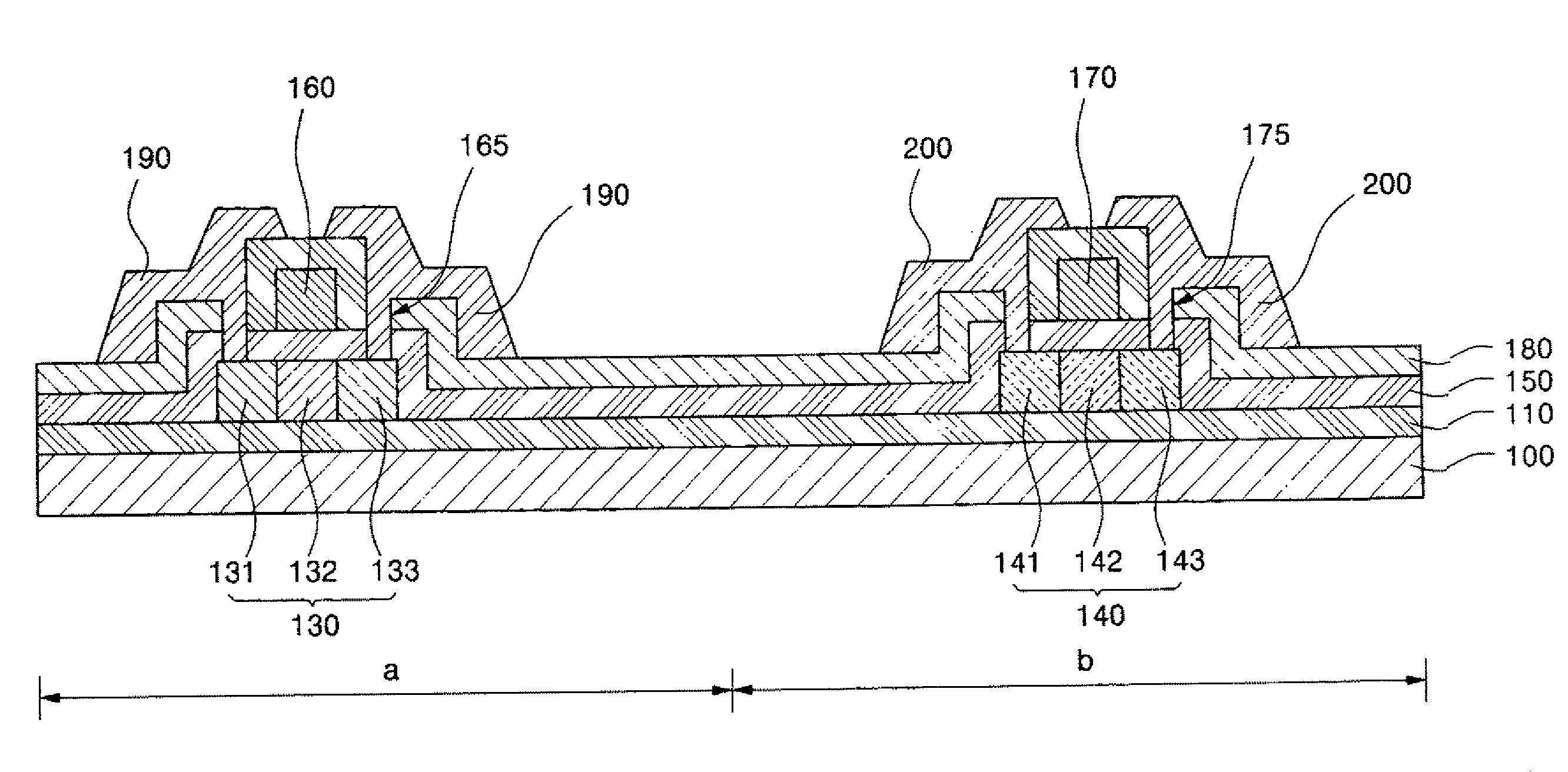
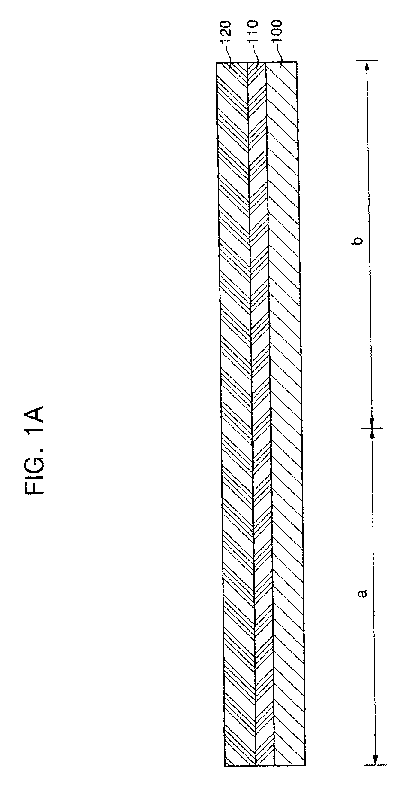
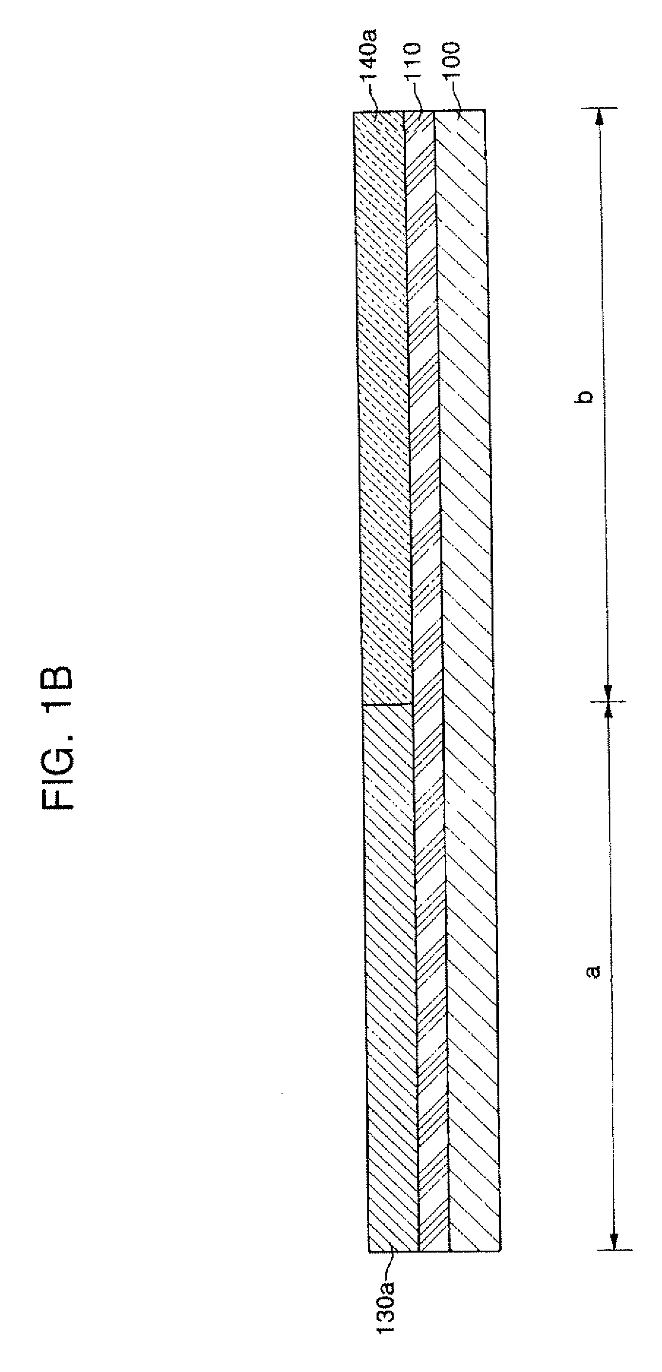
[0022]FIGS. 1A through 1D are cross-sectional views illustrating a fabrication method of a thin film transistor according to an exemplary embodiment of the invention.

[0023]Referring to FIG. 1A, a substrate 100 including a pixel portion (a) and a driver portion (b) is prepared, and a buffer layer 110 is formed on the substrate 100. Here, the substrate 100 may be made of glass, stainless steel, plastic, or the like, and the buffer layer 110 may be made of a silicon nitride layer, a silicon oxide layer or a multi layer of the silicon nitride layer and the silicon oxide layer. Further, the buffer layer 110 prevents moisture or impurities of a lower subst...


PUM

PropertyMeasurementUnit
widthaaaaaaaaaa
widthaaaaaaaaaa
widthaaaaaaaaaa

Abstract

A thin film transistor and a fabrication method thereof, in which one excimer laser annealing (ELA) makes a pixel portion and a driver portion different from each other in surface roughness and grain size. The thin film transistor includes: a substrate including a pixel portion and a driver portion; a first semiconductor layer disposed in the pixel portion and having a first surface roughness; a second semiconductor layer disposed in the driver portion and having a second surface roughness smaller than the first surface roughness; a gate insulating layer formed on the substrate including the first and second semiconductor layers; a first gate electrode placed to correspond to the first semiconductor layer on the gate insulating layer; a second gate electrode placed to correspond to the second semiconductor layer on the gate insulating layer; an interlayer insulating layer formed on the substrate including the first and second gate electrodes; first source and drain electrodes formed on the interlayer insulating layer and electrically connected with the first semiconductor layer; and second source and drain electrodes formed on the interlayer insulating layer and electrically connected with the second semiconductor layer.

Description

CROSS-REFERENCE TO RELATED APPLICATION[0001]This application claims the benefit of Korean Application No. 2006-130186, filed Dec. 19, 2006, in the Korean Intellectual Property Office, the disclosure of which is incorporated herein by reference.BACKGROUND OF THE INVENTION[0002]1. Field of the Invention[0003]An aspect of the present invention relates to a thin film transistor and a fabrication method thereof, and more particularly, to a thin film transistor and a fabrication method thereof in which one excimer laser annealing (ELA) makes a pixel portion and a driver portion different from each other in surface roughness and grain size of a semiconductor layer.[0004]2. Description of the Related Art[0005]Many kinds of display devices are used for displaying an image. Recently, various flat panel display devices have been developed as alternatives to a Braun tube (i.e., a cathode ray tube). Such flat panel display devices are divided into emissive and non-emissive display device types, ...

Claims


Application Information

Patent Timeline
Patent Type & Authority Applications(United States)
IPC IPC(8): H01L29/04H01L21/336
CPCH01L27/12H01L27/1285H01L29/04H01L27/1214H01L21/2026H01L21/02082H01L21/02675H01L29/34
Inventor LEE, HONG-RO
Owner SAMSUNG DISPLAY CO LTD
Why Eureka
Try Eureka