Illumination optical system and exposure apparatus

a technology of illumination optical system and exposure apparatus, which is applied in the direction of microlithography exposure apparatus, printers, instruments, etc., can solve the problems of limited design freedom, difficult to arrange illumination optical system along a straight line, limited usable coating material, etc., and achieve the effect of achieving the effect of effective light source relatively easily and quickly

Inactive Publication Date: 2008-06-19
CANON KK
View PDF12 Cites 9 Cited by
  • Summary
  • Abstract
  • Description
  • Claims
  • Application Information

AI Technical Summary

Benefits of technology

[0011]The present invention is directed to an illumination optical system that obtains a desired effective light source relatively easily and quickly.

Problems solved by technology

It is therefore difficult to arrange the illumination optical system along a straight line, and it is necessary to deflect the optical path using a deflection mirror so as to reduce the size of the exposure apparatus.
The conventional design technology has maintained mirror's transmittance or reflectance fluctuations within the latitude, but recently had difficulties in doing so as the high NA scheme advances in accordance with the fine-processing request.
In addition, a usable coating material is limited for use with the mirror and the light having a wavelength of 250 nm or smaller, and the design freedom is limited accordingly.
Therefore, a desired effective light source distribution could be obtained when no mirror is used, but when the mirror is used, its transmittance and reflectance characteristics preclude a formation of the desired effective light source distribution.
This problem causes a pattern to be exposed with a coherence factor σ different from the optimized one that provides a transfer of the minimum critical dimension (“CD”) of the pattern, thereby preventing the designed resolution CD (in particular minimum CD) from being obtained.
In addition, another problem of “HV difference” occurs which is a difference between horizontal and vertical CDs transferred on a wafer, lowering the yield.
While Japanese Patent Application, Publication No. 2002-093700 proposes a correction of the transmittance by adjusting an angle between two filters each having a discrete transmittance distribution, the angular adjustment requires a measurement of the actual effective light source and a long time.
Another problem is that the discrete transmittance distribution cannot improve the correction accuracy.
On the other hand, Japanese Patent Application, Publication No. 2003-243276 has a purpose to correct the non-uniformity of the transmittance caused by an incident position upon the lens, but does not consider the non-uniformities of the reflectance and transmittance caused by an incident angle upon a mirror.

Method used


Image

  • Illumination optical system and exposure apparatus
  • Illumination optical system and exposure apparatus
  • Illumination optical system and exposure apparatus

Examples


Embodiment Construction

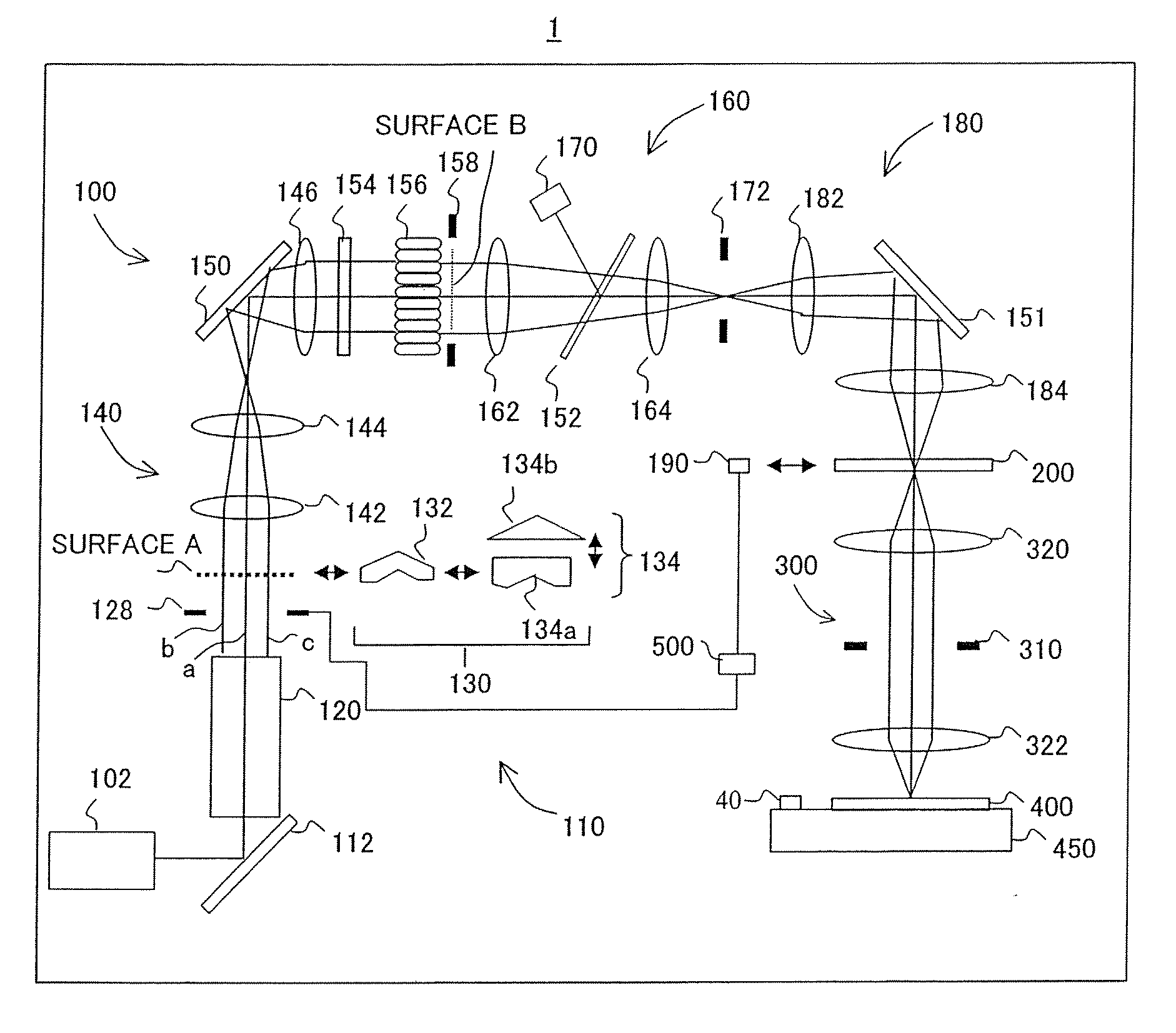
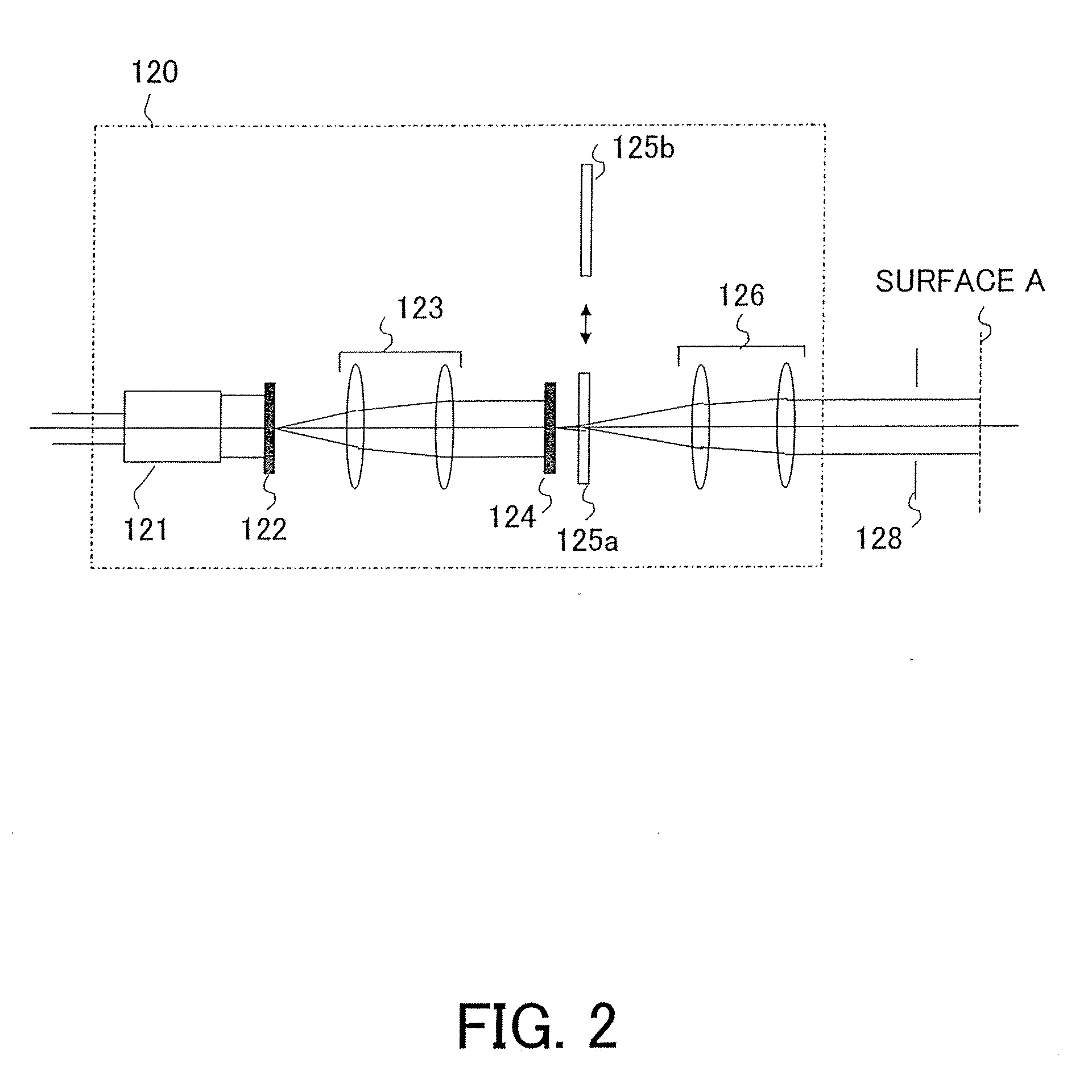
[0037]A description will now be given of an exposure apparatus 1 according to one aspect of the present invention, with reference to the accompanying drawings. Here, FIG. 1 is a schematic structure of the exposure apparatus 1. The exposure apparatus 1 includes, as shown in FIG. 1, an illumination apparatus 100, a reticle 200, a projection optical system 300, a plate 400, a plate stage 450, and a controller 500. The exposure apparatus 100 is a projection exposure apparatus that exposes a circuit pattern of the reticle 200 onto the plate 400 in a step-and-scan manner. However, the present invention is applicable to a step-and-scan exposure apparatus.

[0038]The illumination apparatus illuminates the reticle 200 that has a circuit pattern to be transferred, and includes a light source section 102 and an illumination optical system 110.

[0039]The light source section 102 may use as a light source, for example, an ArF excimer laser with a wavelength of about 193 nm, a KrF excimer laser of a...


PUM

PropertyMeasurementUnit
wavelengthaaaaaaaaaa
transmittanceaaaaaaaaaa

Abstract

An illumination optical system that is used for an exposure apparatus that includes a mirror and exposes an object, illuminates a surface to be illuminated using light from a light source, and includes a filter member arranged at a position that substantially has a Fourier transform relationship with the surface to be illuminated, the filter member including a transmittance distribution preset to correct a non-uniformity of a transmittance distribution of the illumination optical system caused by the mirror.

Description

[0001]This application is a continuation of prior application Ser. No. 11 / 144,710, filed Jun. 2, 2005, to which priority under 35 U.S.C. §120 is claimed. This application also claims a benefit of priority based on Japanese Patent Application Nos. 2004-166552, filed on Jun. 4, 2004, and 2005-116585, filed on Apr. 14, 2005, both of which are hereby incorporated by reference herein in their entirety as if fully set forth herein.BACKGROUND OF THE INVENTION[0002]The present invention relates to an illumination optical system, and more particularly to control over an incident angle distribution or light distribution characteristic (also referred to as “effective light source” and “a distribution”) on a surface to be illuminated (“target surface”). The inventive illumination optical system is suitable for an exposure apparatus for the micro-lithography used to manufacture fine patterns such as semiconductor devices, liquid crystal devices (“LCDs”) and magnetic materials.[0003]A projection ...

Claims


Application Information

Patent Timeline
Patent Type & Authority Applications(United States)
IPC IPC(8): G03B27/72G03F7/20
CPCG03F7/70083G03F7/70566G03F7/70191G03F7/70108
Inventor SHIOZAWA, TAKAHISAGOTO, YOSHIO
Owner CANON KK
Why Eureka
Try Eureka