Semiconductor memory device and method of manufacturing the same

a memory device and semiconductor technology, applied in semiconductor devices, electrical devices, instruments, etc., can solve the problems of rram and physical limit due to lithography limit, and achieve the same problems as rram

Inactive Publication Date: 2008-06-26
KK TOSHIBA
View PDF1 Cites 190 Cited by
  • Summary
  • Abstract
  • Description
  • Claims
  • Application Information

AI Technical Summary

Problems solved by technology

However, the PRAM has the following problems.
Specifically, there is a physical limit due to lithography limit to achieve the scale reduction of the plan direction.
Moreover, RRAM has the same problems as above.

Method used


Image

  • Semiconductor memory device and method of manufacturing the same
  • Semiconductor memory device and method of manufacturing the same
  • Semiconductor memory device and method of manufacturing the same

Examples


first embodiment

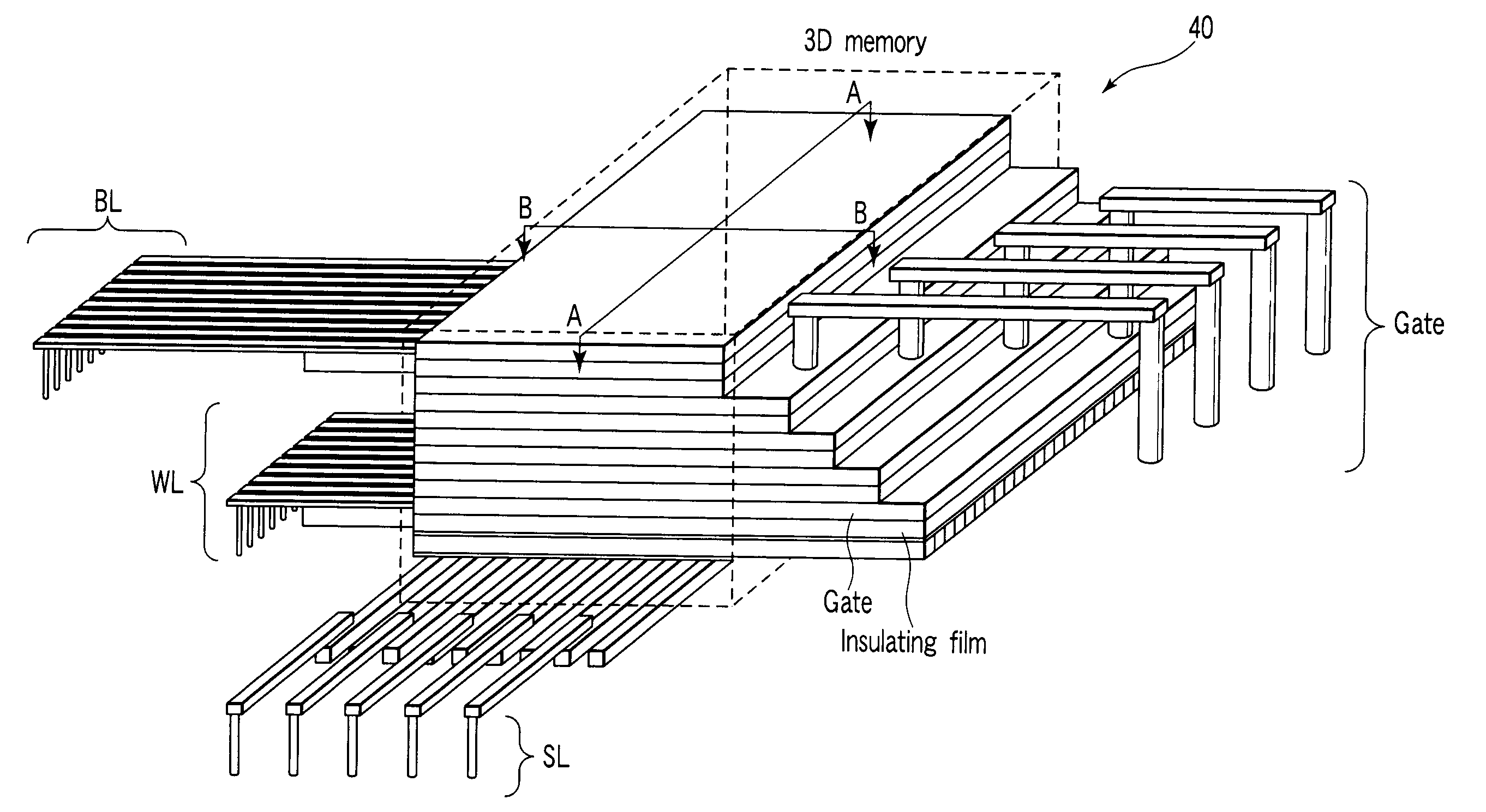
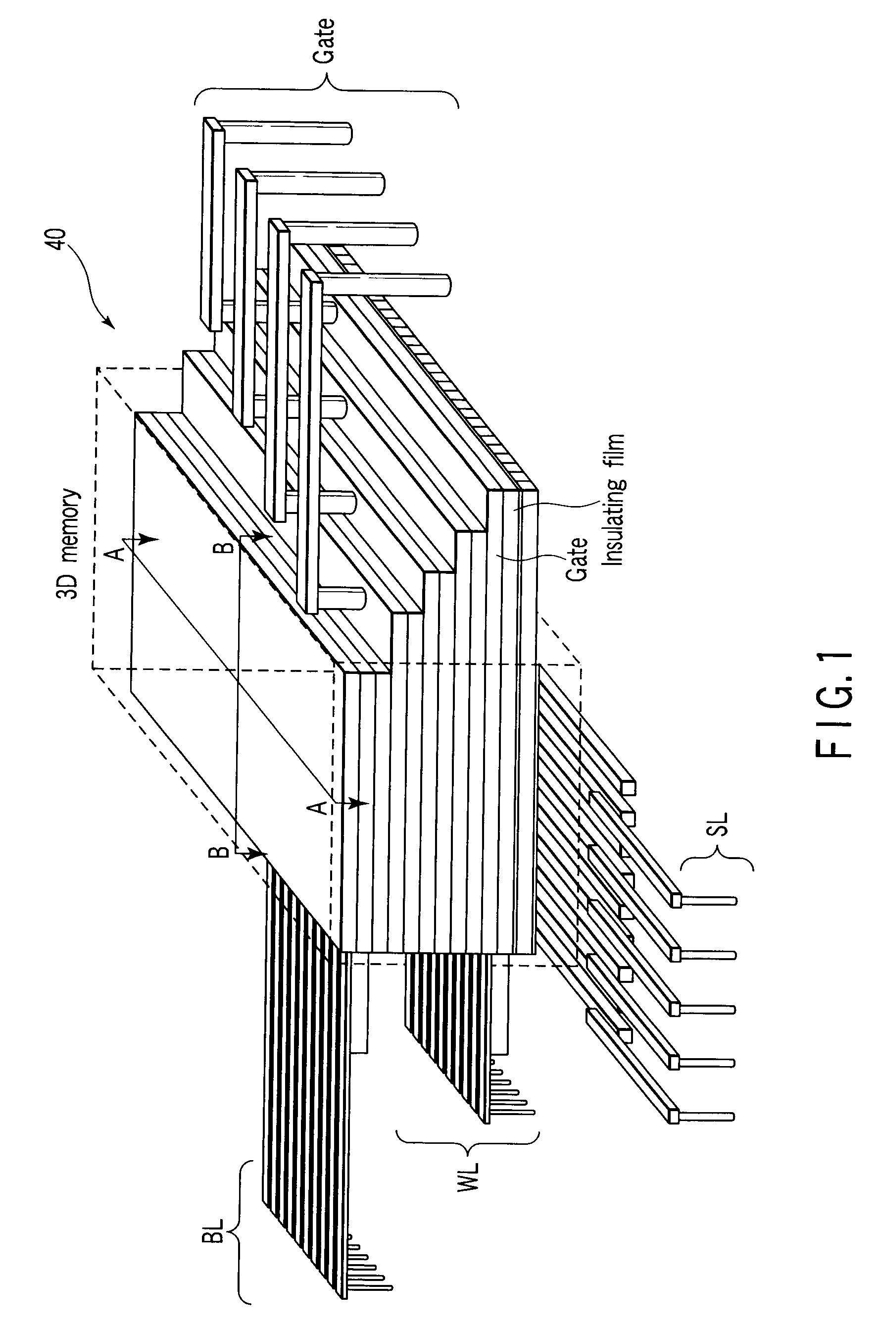
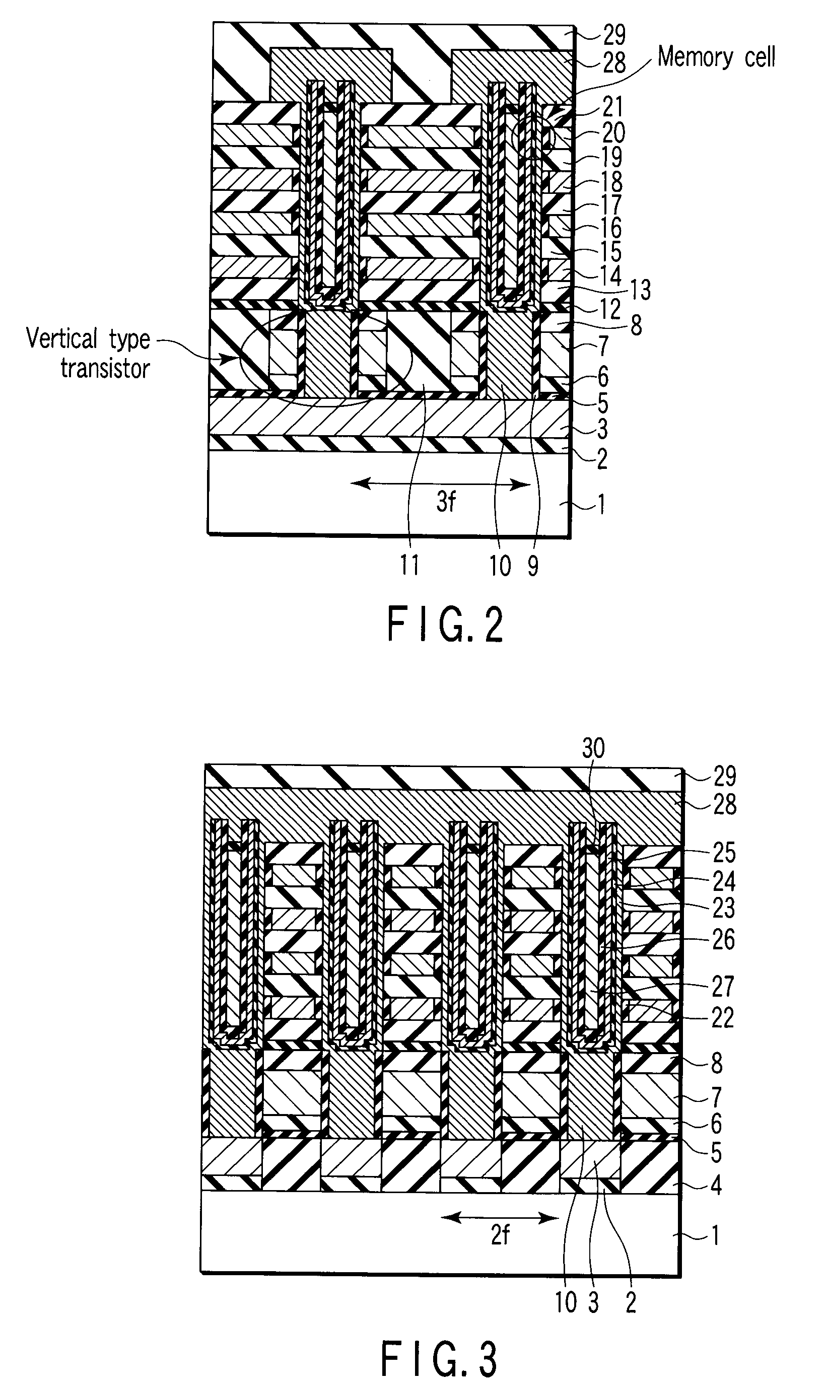
[0088]A semiconductor memory device and a method of manufacturing the same according to a first embodiment of the present invention will be hereinafter described with reference to the accompanying drawings. FIG. 1 is a perspective view showing a structure of a semiconductor memory device according to a first embodiment of the present invention. FIG. 2 is a cross-sectional view of the semiconductor memory device shown in FIG. 1, taken along the line A-A of FIG. 1. FIG. 3 is a cross-sectional view of the semiconductor memory device shown in FIG. 1, taken along the line B-B of FIG. 1. FIG. 4 is a cross-sectional view of a memory cell portion of the semiconductor memory device according to the first embodiment of the present invention. FIG. 5 is a cross-sectional view showing one memory cell of the semiconductor memory device shown in FIG. 4. FIG. 6 is a view showing an equivalent circuit diagram of the semiconductor memory device shown in FIG. 4. In the first embodiment, a plurality of...

second embodiment

[0126]A semiconductor memory device and a method of manufacturing the same according to a second embodiment of the present invention will be hereinafter described with reference to the accompanying drawings. FIG. 48 is a cross-sectional view of a memory cell portion of a semiconductor memory device according to a second embodiment of the present invention. FIG. 49 is a cross-sectional view showing one memory cell of the semiconductor memory device shown in FIG. 48. FIG. 50 is a view showing an equivalent circuit diagram of the semiconductor memory device shown in FIG. 48. In the second embodiment, the memory cell of the PRAM is stacked on a semiconductor substrate to form a three-dimensional memory cell.

[0127]In the following description, the same reference numbers are used to designate portions identical to the first embodiment, and different portions only will be described.

[0128]As shown in FIG. 48 to FIG. 50, in the memory cell portion of the RRAM (resistive change random access ...


PUM


Abstract

A semiconductor memory device is disclosed, which includes a first memory cell array formed on a semiconductor substrate and composed of a plurality of memory cells stacked in layers each having a characteristic change element and a vertical type memory cell transistor connected in parallel to each other, a plurality of second memory cell arrays formed on the semiconductor substrate and having the same structure as the first memory cell array, and arranged in an X direction with respect to the first memory cell array, and a plurality of third memory cell arrays formed on the semiconductor substrate and having the same structure as the first memory cell array, and arranged in a Y direction with respect to the first memory cell array, wherein a gate voltage is applied to gates of the vertical type memory cell transistors of the first to third memory cell arrays in a same layer.

Description

CROSS-REFERENCE TO RELATED APPLICATIONS[0001]This application is based upon and claims the benefit of priority from prior Japanese Patent Application No. 2006-349538, filed Dec. 26, 2006, the entire contents of which are incorporated herein by reference.BACKGROUND OF THE INVENTION[0002]1. Field of the Invention[0003]The present invention relates to a semiconductor memory device, and to a method of manufacturing the same.[0004]2. Description of the Related Art[0005]A next-generation non-volatile memory has been developed, and has the following features. The next-generation non-volatile memory is rewritable at high speed as compared with conventional EEPROM and flash memory. In addition, the number of rewritable times is larger than five digits. The next-generation non-volatile memory is developed for the purpose of realizing the capacity equivalent to DRAM, speed and cost. For example, FeRAM (Ferroelectric Random Access Memory), MRAM (Magnetic Random Access Memory), PRAM (Phase chang...

Claims


Application Information

Patent Timeline
Patent Type & Authority Applications(United States)
IPC IPC(8): H01L27/105H01L21/8239H01L45/00
CPCH01L45/04H01L45/06H01L45/1233H01L45/141G11C2213/75H01L45/146H01L27/2454H01L27/2481G11C2213/71H01L45/144H10B63/34H10B63/84H10N70/20H10N70/882H10N70/231H10N70/8828H10N70/8833H10N70/826
Inventor TANAKA, HIROYASUKATSUMATA, RYOTAAOCHI, HIDEAKIKITO, MASARUKIDOH, MASARUSATO, MITSURU
Owner KK TOSHIBA
Why Eureka
Try Eureka