Semiconductor device having opposite-polarity region under channel

a technology of opposite polarity and semiconductor devices, which is applied in the direction of semiconductor devices, basic electric elements, electrical appliances, etc., can solve the problems of increasing the standby current of the device, increasing the power consumption of the semiconductor device with the increasing degree of integration, and increasing the amount of leakage current between the drain and the sour

Inactive Publication Date: 2000-12-19
RICOH KK
View PDF9 Cites 98 Cited by
  • Summary
  • Abstract
  • Description
  • Claims
  • Application Information

AI Technical Summary

Problems solved by technology

Although metal-oxide-semiconductor field effect transistors (MOS FET) are advantageous for integration, the power consumption of the semiconductor devices increases with the increasing degree of integration.
In conventional semiconductor devices, however, there has arisen a problem in that some amount of leakage currents persist between the drain and source even at zero gate voltage.
In the semiconductor devices with either one of the above-mentioned conventional structures, however, there has remained a problem that, because of a short distance between drain and substrate, some amount of leakage currents still persist between drain and substrate when a voltage is applied to the drain even at zero gate voltage, thereby resulting in the increase of standby currents of the devices.

Method used


Image

  • Semiconductor device having opposite-polarity region under channel
  • Semiconductor device having opposite-polarity region under channel
  • Semiconductor device having opposite-polarity region under channel

Examples


second embodiment

Referring to FIGS. 3a and 3b, the present invention is described. In the following description, steps different from those previously described are primarily detailed.

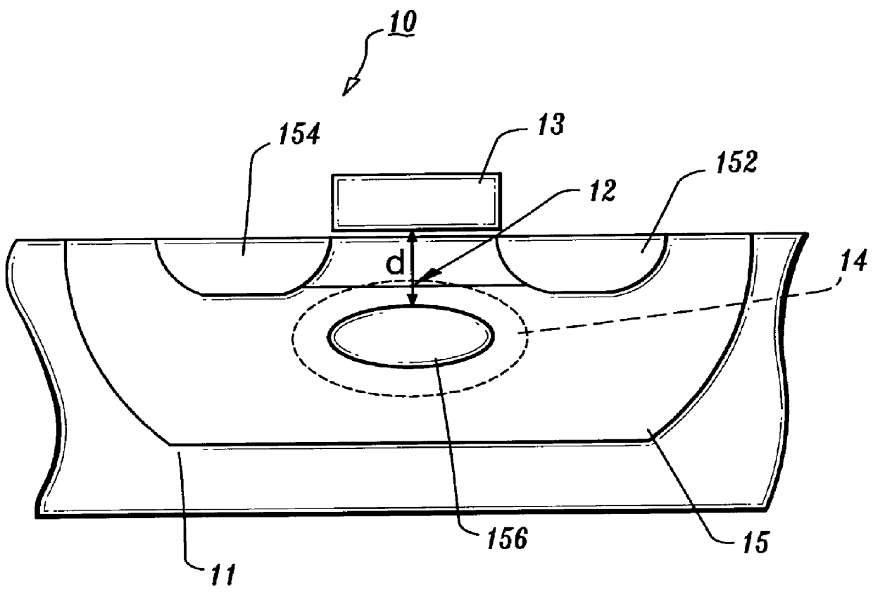
As will be described hereinbelow, the manufacturing of the second embodiment is characterized by a step of implanting ions of a conductive type opposite to that of a well region 15 (i.e., n-type) incident normal through a gate electrode 13 previously disposed, thereby forming an opposite-polarity region 156 which is surrounded by a well region 15 and situated under the channel, source, and drain regions, as shown in FIG. 2b. In addition, the opposite-polarity region 156 can induce a second depleted region 14 as aforementioned, thereby making the drain current more responsive to the applied gate bias voltage.

Referring to FIG. 3a, in the process for the second embodiment, (1) prior to the formation of a gate electrode 13, a well region 15 is formed, (2) an n.sup.- source region 152 and an n.sup.- drain region 154 are sub...

third embodiment

Referring to FIGS. 4a through 4c, the present invention is described. In the following description, steps different from those previously described are primarily detailed with the same reference numerals representing the same or like elements.

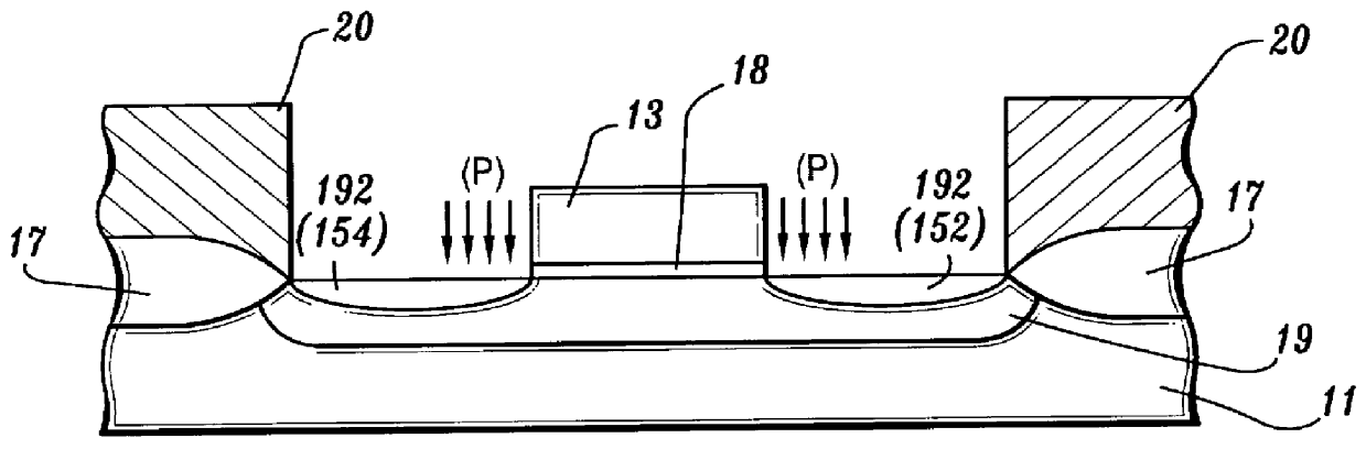
The manufacturing of the third embodiment is characterized by the steps of (1) prior to the formation of a gate electrode 13, forming a second well region 24 which is situated deep under a channel region 19, and (2) subsequent to the formation of the gate electrode 13 and a first well region under the channel region 19, forming a well region 15 and an opposite-polarity region 156 which has a conductive type opposite to that of the well region 15 and surrounded by a well region 15, as shown FIG. 4c.

By utilizing the above-mentioned process of forming the second well 24 and the (first) well 15, an opposite-polarity region 156 and a concurrent second depleted region 14 (FIG. 1) are formed adjacent to the channel region and between the second well 2...

first embodiment

MOS transistor characteristic measurements were obtained for a device according to the present invention and for comparative first and second prior art devices. The measurements were carried out by (1) applying 1.5 volts to drain, (2) adjusting the potential of the gate and the substrate at 0 volts, and (3) measuring both values of the substrate and drain currents with increasing voltages applied to the gate. From the gate voltage and current values obtained, a sub-threshold coefficient or S-factor (mV / decade) is calculated. The S-factor represents a gate bias voltage value needed to increase source-drain current by one order of magnitude.

The smaller the substrate current, the more preferable the device characteristics. In addition, the smaller the S-factor, the more steep the increase of the drain current with the increase of gate voltage. For the MOS field effect transistor 10 of the first embodiment, a substrate current and an S-factor were obtained as 1 pA at most and 75, respec...


PUM


Abstract

A semiconductor device and fabrication method thereof are provided, which include an opposite-polarity region formed in a predetermined location under a gate channel region, having a conductive property opposite to that of a surrounding well region. The gate voltage is controlled so that a second depleted layer region is induced concurrently with the opposite-polarity region by the applied gate voltage and can be coupled with a first depleted region which is formed under the channel region and is controllable by the applied gate voltage. In this structure of the semiconductor device, drain current of the device is rendered more responsive to the applied gate voltage, and leakage currents at a certain applied drain voltage and at zero gate voltage are reduced, thereby reducing the standby currents of the semiconductor device.

Description

1. Field of the InventionThis invention relates to a semiconductor device having a transistor of MOS structure and an opposite-polarity region under a channel region of the transistor, and a method of fabricating the same semiconductor device.2. Description of the Related ArtAs integration of semiconductor devices advances toward higher density, miniaturization of the devices continues. Although metal-oxide-semiconductor field effect transistors (MOS FET) are advantageous for integration, the power consumption of the semiconductor devices increases with the increasing degree of integration.Accordingly, semiconductor devices having MOS structure are suitable when higher integration and low power consumption are both required. In addition, the demands of gate oxide reliability requires that the supply voltage be reduced for the semiconductor devices.To implement the low supply voltage for semiconductor devices, it is necessary for a transistor to have a low threshold voltage V.sub.th ...

Claims


Application Information

Patent Timeline
Patent Type & Authority Patents(United States)
IPC IPC(8): H01L21/02H01L21/70H01L21/265H01L21/336H01L21/8238H01L29/10H01L29/02
CPCH01L21/26586H01L29/66537H01L29/1083H01L21/823807
Inventor KAWASHIMA, IKUE
Owner RICOH KK
Why Eureka
Try Eureka