Semiconductor light-emitting structure and graded-composition substrate providing yellow-green light emission

a technology of semiconductors and light-emitting structures, applied in the direction of semiconductor devices, basic electric elements, electrical equipment, etc., can solve the problems of low green emission of light-emitting devices including aluminum in their active region, light-emitting devices such as leds on small lattice constant substrates, and (al)ingan-based light-emitting devices (leds) on gaas substrates

Inactive Publication Date: 2008-06-26
MASSACHUSETTS INST OF TECH
View PDF54 Cites 50 Cited by
  • Summary
  • Abstract
  • Description
  • Claims
  • Application Information

AI Technical Summary

Problems solved by technology

Currently, light-emitting semiconductor technology lacks a commercially viable materials system for green emission, as no green group III-V semiconductor lasers with pure emission (e.g., not frequency doubled) are known to have been previously demonstrated.
Light-emitting devices including aluminum in their active region, such as (Al)InGaN-based light-emitting devices (LEDs) on small lattice constant substrates (e.g., sapphire) and AlInGaP LEDs on GaAs substrates (e.g., epitaxially grown on GaAs substrates), lack the efficiency of other emitters.
Materials that currently dominate the LED market have not demonstrated very good performance in the yellow-green part of the spectrum, as illustrated in FIG. 1.
However, despite the very short minority carrier lifetimes induced by the quantum wells, the high dislocation density present in GaN layers combined with the inability to add enough indium (In) to form deep quantum wells (due to InGaN—GaN lattice-mismatch and thermodynamic constraints) can result in lower efficiency as compared with typical blue emission performance.
As the emitted wavelength becomes smaller (e.g., greener, rather than redder), larger band gap active regions must be used, reducing the available electronic and optical confinement in the devices and thus making them less efficient.
Green-emitting AlInGaP devices that are lattice-matched to GaAs have poor internal quantum efficiency due to the proximity of the indirect-direct bandgap crossover at the compositions of interest, as well as due to oxygen-related defects.
These 500-600 nm devices often have very poor color purity, leading to an undersaturated appearance.
This is a particular problem in the green region, where a deviation of as little as 2 nm may be discernable to the human eye.
The prediction of the electronic structure of AlInGaP alloys is quite complex.
Especially with compositions of the alloy far away from the lattice constant of GaAs, it is currently difficult to accurately predict the electronic structure of light-emitting designs.

Method used


Image

  • Semiconductor light-emitting structure and graded-composition substrate providing yellow-green light emission
  • Semiconductor light-emitting structure and graded-composition substrate providing yellow-green light emission
  • Semiconductor light-emitting structure and graded-composition substrate providing yellow-green light emission

Examples


Embodiment Construction

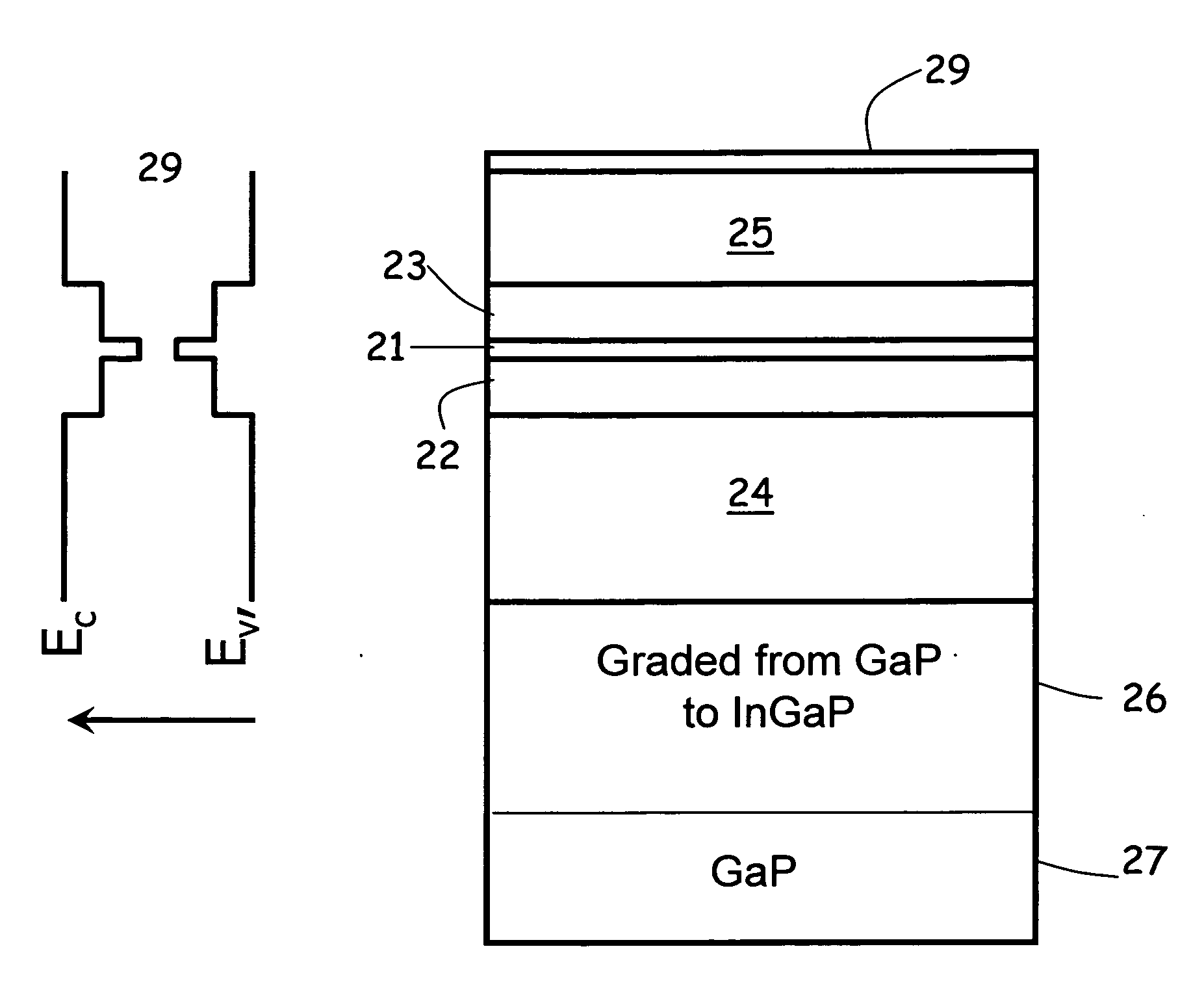
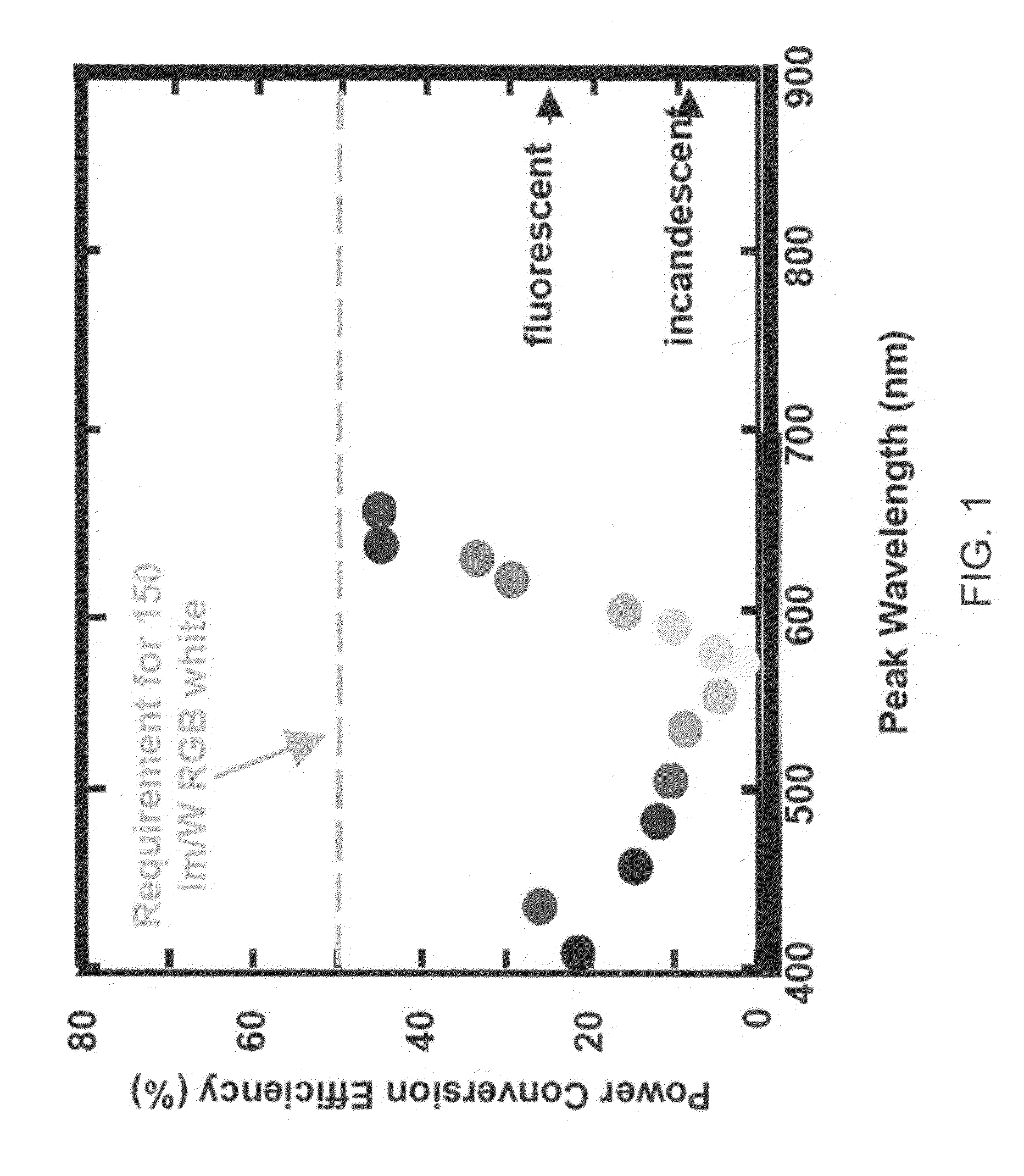
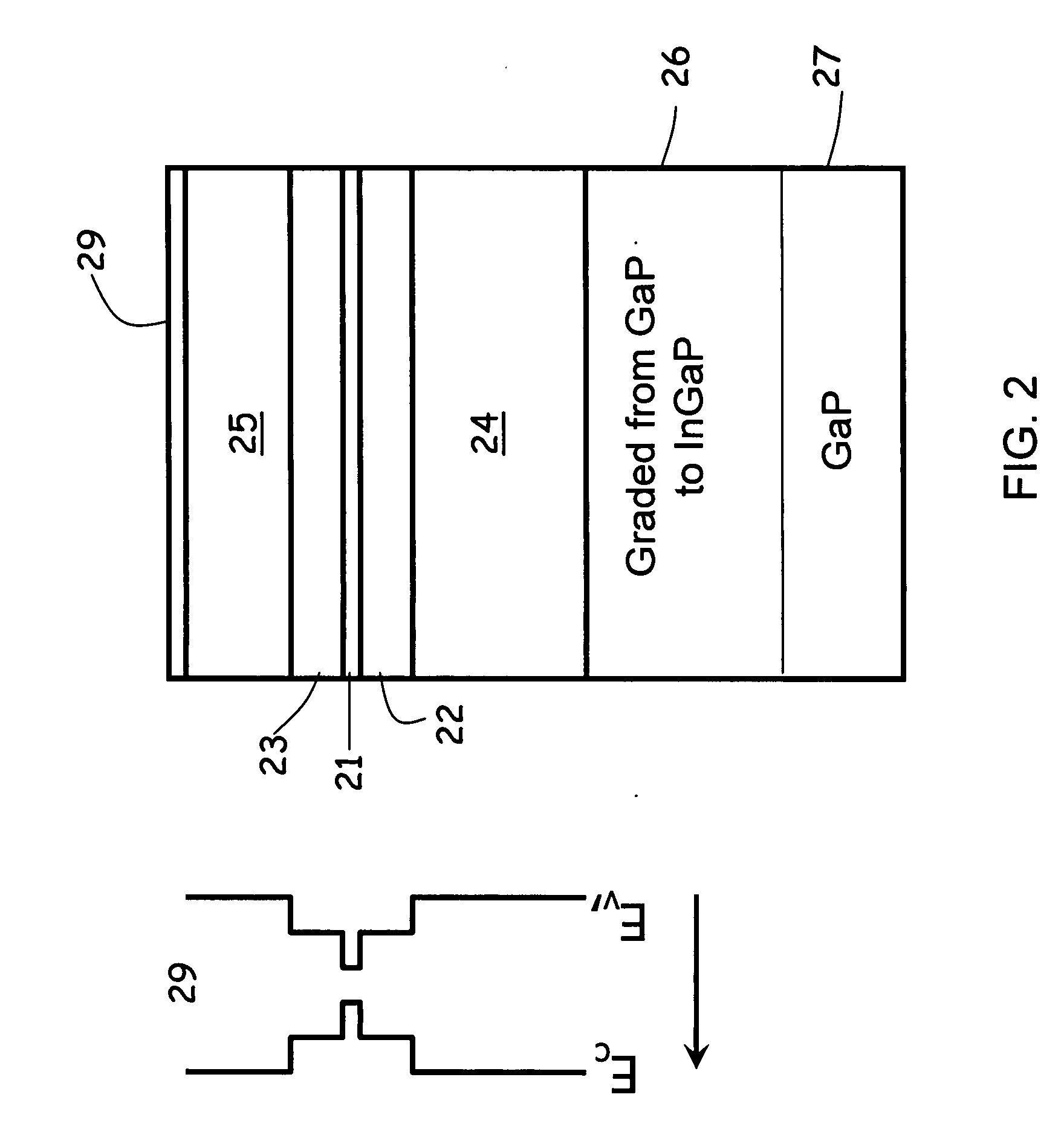
[0025]Applicants have appreciated that by relaxing the constraint that the light-emitting semiconductor material (e.g., AlInGaP or InGaP) be lattice-matched to GaAs, it is possible to use compositions of these semiconductor materials with a larger band gap in the yellow-green portion of the visible electromagnetic spectrum. In inorganic materials systems, Applicants believe the inability to achieve efficient yellow-green emission may be a result of a lattice-mismatch problem, as the lattice constant of AlInGaP and InGaP desirable for yellow-green light emission is different from that of common substrate materials, such as GaAs. By using compositions of AlInGaP or InGaP that are not lattice-matched to GaAs, high-efficiency yellow-green emission can be achieved by choosing compositions of these materials that provide more desirable electrical and optical confinement. One difficulty with this approach, however, has been the prevalence of crystal defects resulting from the growth of a l...


PUM


Abstract

Semiconductor light-emitting structures are shown on engineered substrates having a graded composition. The composition of the substrate may be graded to achieve a lattice constant on which a yellow-green light-emitting semiconductor material may be disposed. In some embodiments, the structure may be substantially free of aluminum.

Description

RELATED APPLICATIONS[0001]This application claims the benefit under 35 U.S.C. §119(e) of U.S. Provisional Application Ser. No. 60 / 816,933, entitled “AL-FREE INGAP-BASED LASER AND LED HETEROSTRUCTURE ON A LATTICE MISMATCHED SUBSTRATE,” filed on Jun. 28, 2006, which is hereby incorporated by reference in its entirety.FEDERALLY SPONSORED RESEARCH[0002]This invention was made with U.S. Government support under contract B-12-M06-52. The U.S. Government may have certain rights to this invention.BACKGROUND[0003]1. Technical Field[0004]The techniques described herein relate to semiconductor light-emitting structures capable of emitting light in the yellow-green portion of the visible electromagnetic spectrum, substrates on which such structures may be formed, and methods for fabricating such structures.[0005]2. Discussion of Related Art[0006]Currently, light-emitting semiconductor technology lacks a commercially viable materials system for green emission, as no green group III-V semiconduct...

Claims


Application Information

Patent Timeline
Patent Type & Authority Applications(United States)
IPC IPC(8): H01L33/00H01L33/12H01L33/30
CPCH01L33/30H01L33/12
Inventor MORI, MICHAEL J.FITZGERALD, EUGENE A.
Owner MASSACHUSETTS INST OF TECH
Why Eureka
Try Eureka