III-Nitride Compound Semiconductor Light Emitting Device

Inactive Publication Date: 2008-06-26
EPIVALLEY
View PDF5 Cites 42 Cited by
  • Summary
  • Abstract
  • Description
  • Claims
  • Application Information

AI Technical Summary

Benefits of technology

[0029]According to the present invention as described above, electrons can be effectively supplied to the active layer 30, and at the same time, the lattice mismatch between the lower contact layer 20 and th

Problems solved by technology

The above-described prior III-nitride compound semiconductor light emitting device has a problem in that the lattice mismatch between the lower contact layer 20 and the active layer 30 is very large.
Particularly, when the piezoelectric phenomenon occurs within the active layer 30, a change of the energy band shape of the active layer 30 will be caused, resulting in the distortion of the wave functions of holes and electrons, thus reducing light emitting efficiency in the active layer 30.
Meanwhile, as the concentration of n-type dop

Method used


Image

  • III-Nitride Compound Semiconductor Light Emitting Device
  • III-Nitride Compound Semiconductor Light Emitting Device
  • III-Nitride Compound Semiconductor Light Emitting Device

Examples


Embodiment Construction

[0041]Hereinafter, the present invention will be described in detail with reference to the accompanying drawings. In the drawings, the same reference numerals as those in FIG. 1 represent elements performing the same functions, and a duplicate description thereof will be omitted.

[0042]The following embodiments are provided for a better understanding of the present invention and it will be obvious to any person skilled in the art that many modifications to these embodiments can be made within technical concept of the present invention. Accordingly, it should not be construed that the scope of the present invention is not limited to or by these embodiments.

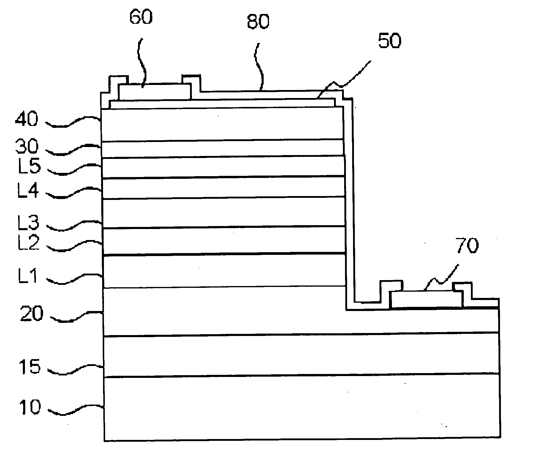
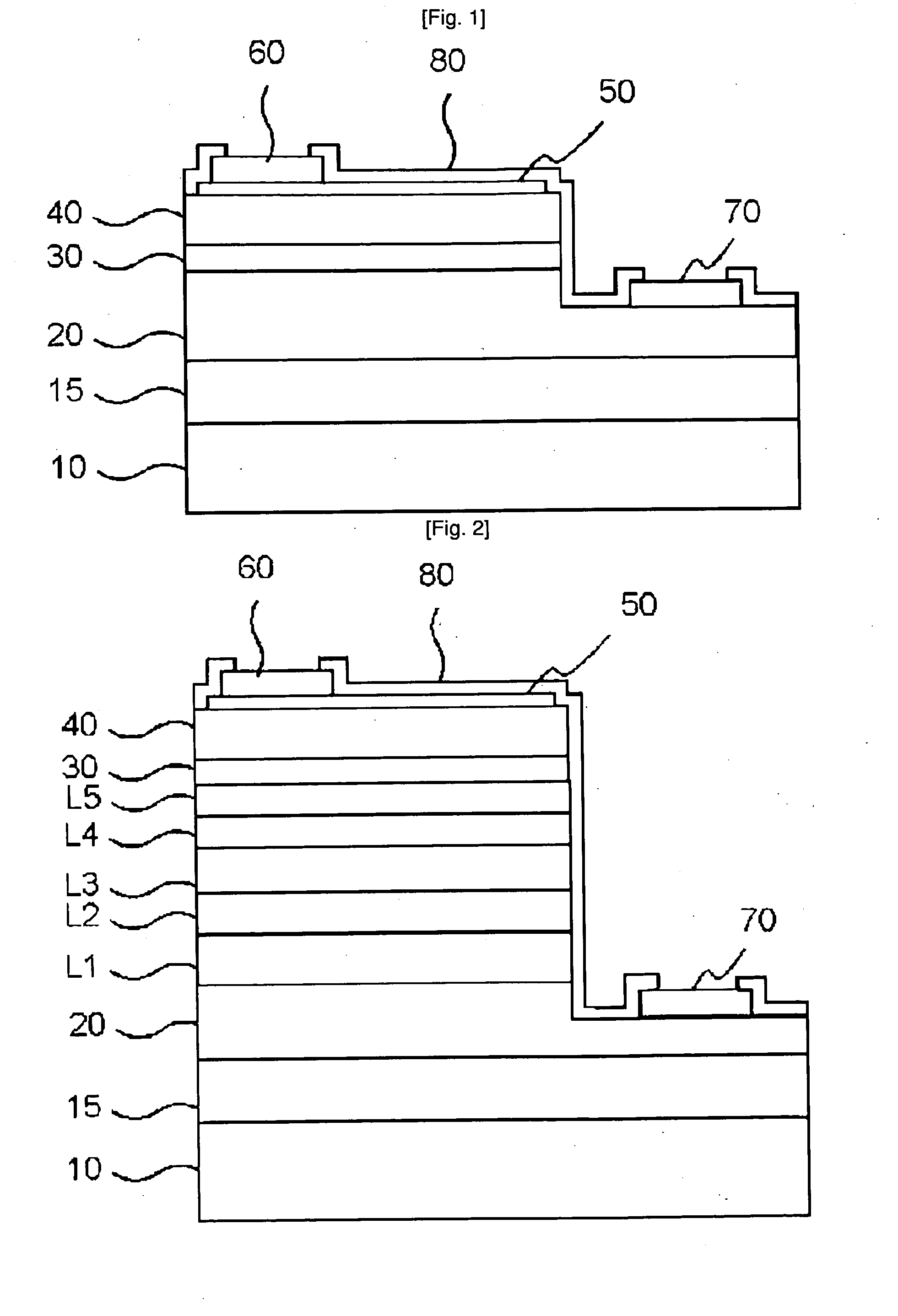
[0043]FIG. 2 is a cross-sectional view illustrating a III-nitride compound semiconductor light emitting device according to an embodiment of the present invention.

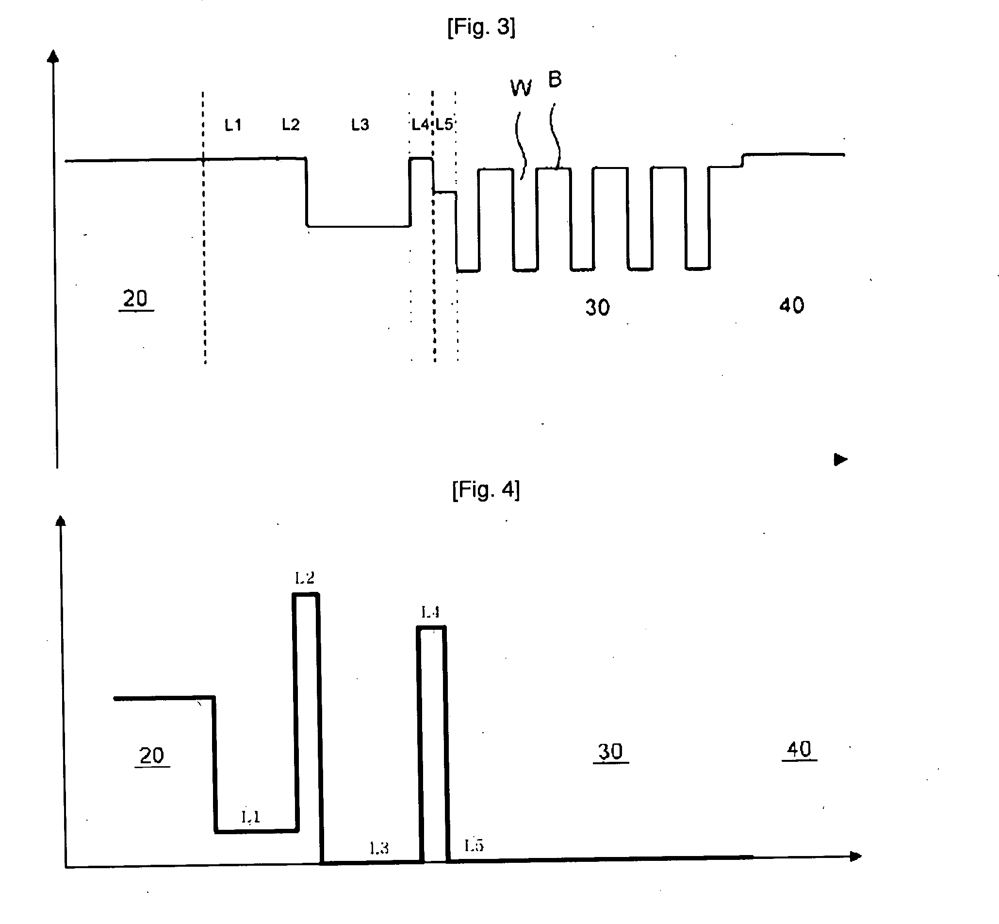
[0044]Referring to FIG. 2, between the lower contact layer 20 and the active layer 30, the lattice mismatch-reducing layer L3 made of undoped InxGa1-xN to reduce strain ca...


PUM


Abstract

The present invention provides a III-nitride compound semiconductor light emitting device comprising an active layer (30) which emits light and is interposed between a lower contact layer (20) made of n-GaN and an upper contact layer (40) made of p-GaN, in which a sequential stack of a lattice mismatch-reducing layer L3 made of InxGa1-xN, an electron supply layer L4 made of n-GaN or n-AlyGa1-yN and a crystal restoration layer L5 made of InzGa1-zN is interposed between the lower contact layer and the active layer, and further comprising an electron acceleration layer L1 made of n-GaN or undoped GaN and a heterojunction electron barrier-removing layer L2, thereby the lattice mismatch between the lower contact layer (20) and the active layer (30) can be reduced.

Description

TECHNICAL FIELD[0001]The present invention relates to a III-nitride compound semiconductor light emitting device, and more particularly, to a III-nitride compound semiconductor light emitting device in which the lattice mismatch between an active layer and a lower contact layer made of n-GaN can be reduced and a reduction in thin film quality caused by the doping of an n-type dopant can be prevented.BACKGROUND ART[0002]FIG. 1 is a cross-sectional view for illustrating a III-nitride compound semi-conductor light emitting device according to the prior art.[0003]Referring to FIG. 1, the prior III-nitride compound semiconductor light emitting device is fabricated in the following manner. The buffer layer 15 made of undoped GaN, the lower contact layer 20 made of n-GaN, the active layer 30 with a single-quantum-well structure or a multiple-quantum-well structure, and the upper contact layer 40 made of p-GaN, are sequentially deposited on the sapphire substrate 20. Then, mesa etching is p...

Claims


Application Information

Patent Timeline
IPC IPC(8): H01L33/00H01L33/06H01L33/12H01L33/14H01L33/32
CPCH01L33/06H01L33/12H01L33/14H01L33/32
Inventor YOO, TAE KYUNGPARK, EUN HYUN
Owner EPIVALLEY
Why Eureka
Try Eureka