Light emitting diode having algan buffer layer and method of fabricating the same

a technology buffer layers, which is applied in the direction of transportation and packaging, acoustic signal devices, semiconductor devices, etc., can solve the problems of higher defect density of gan-based buffer layers and higher defect density of layers, so as to reduce lattice mismatch, reduce the defect density of light emitting diodes, the effect of reducing the defect density

Active Publication Date: 2010-02-11
SEOUL VIOSYS CO LTD
View PDF9 Cites 8 Cited by
  • Summary
  • Abstract
  • Description
  • Claims
  • Application Information

AI Technical Summary

Benefits of technology

[0010]The present invention is conceived to solve the aforementioned problems. Accordingly, an object of the present invention is to lower a defect density of a light emitting diode by reducing lattice mismatch between a substrate and a GaN-based semiconductor layer.
[0024]According to the present invention, lattice mismatch between a substrate and a GaN-based semiconductor layer can be reduced due to an AlxGa1-xN (0≦x≦1) buffer layer having the composition ratio x of Al decreasing from the substrate to the GaN-based semiconductor layer, thereby lowering a defect density of a light emitting diode.

Problems solved by technology

However, the conventional light emitting diode has problems in that the GaN-based buffer layer has a higher defect density due to a difference in lattice constant between the sapphire substrate and the GaN-based buffer layer grown on the sapphire substrate, and the doped GaN-based conductive semiconductor layer grown on the GaN-based buffer layer also has a higher defect density due to high stress.

Method used


Image

  • Light emitting diode having algan buffer layer and method of fabricating the same
  • Light emitting diode having algan buffer layer and method of fabricating the same
  • Light emitting diode having algan buffer layer and method of fabricating the same

Examples


Embodiment Construction

[0032]Hereinafter, preferred embodiments of the present invention will be described in detail with reference to the accompanying drawings.

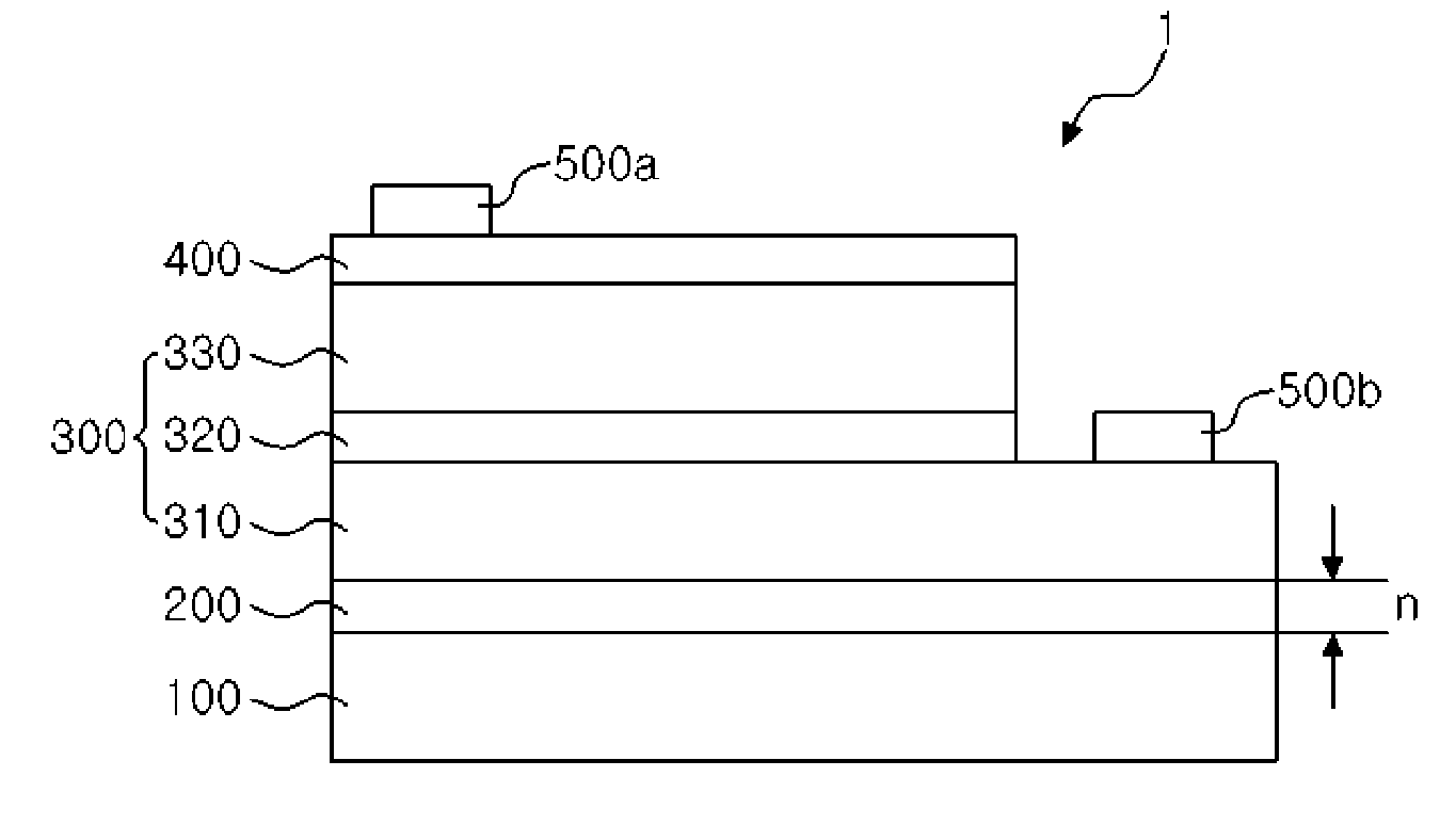
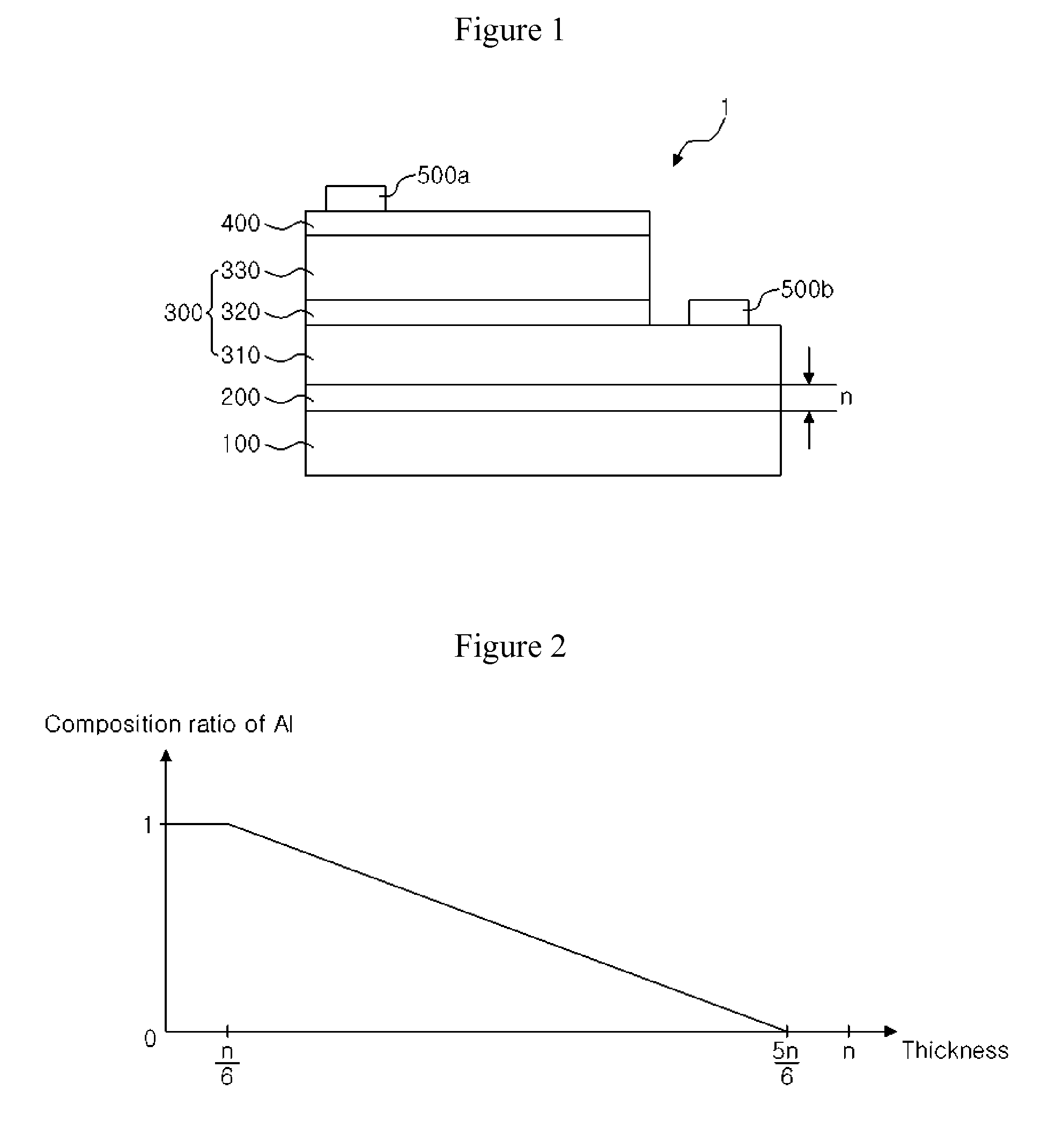
[0033]FIG. 1 is a sectional view of a light emitting diode according to an embodiment of the present invention.

[0034]Referring to FIG. 1, the light emitting diode 1 according to the embodiment of the present invention includes a sapphire substrate 100, an AlxGa1-xN (0≦x≦1) buffer layer 200, a first conductive semiconductor layer 310, an active layer 320, a second conductive semiconductor layer 330, a transparent electrode 400, and electrode pads 500a and 500b.

[0035]The sapphire substrate 100 is made of sapphire with good stability, and the AlxGa1-xN buffer layer 200 is formed on the sapphire substrate 100.

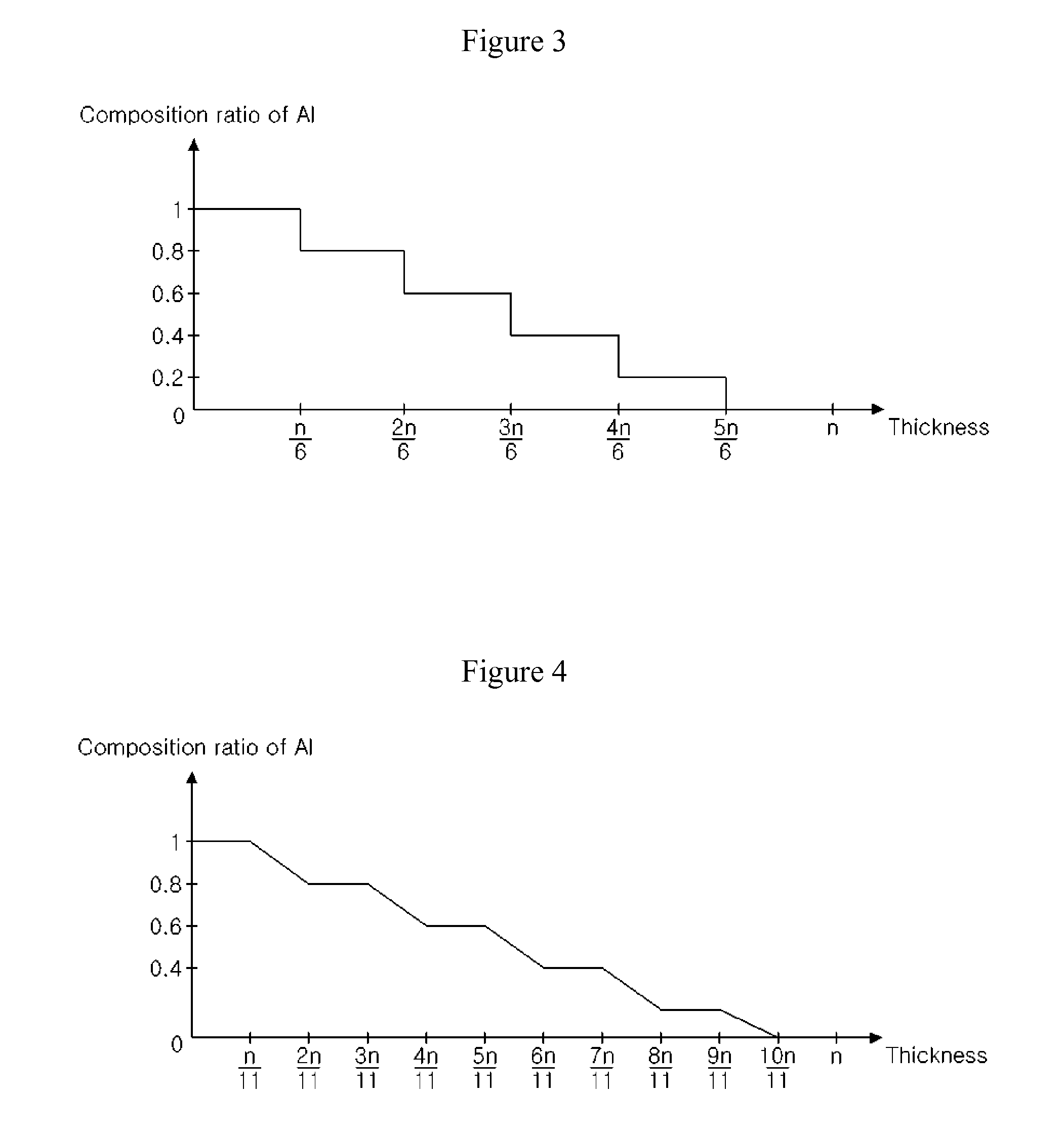
[0036]The AlxGa1-xN (0≦x≦1) buffer layer 200 is interposed between the sapphire substrate and the first conductive semiconductor layer 310 (e.g., a GaN-based semiconductor layer or the like). The composition ratio x of Al decreases from the sapp...


PUM


Abstract

The present invention relates to a light emitting diode having an AlxGa1-xN buffer layer and a method of fabricating the same, and more particularly, to a light emitting diode having an AlxGa1-xN buffer layer, wherein between a substrate and a GaN-based semiconductor layer, the AlxGa1-xN (0≦x≦1) buffer layer having the composition ratio x of Al decreasing from the substrate to the GaN-based semiconductor layer is interposed to reduce lattice mismatch between the substrate and the GaN-based semiconductor layer, and a method of fabricating the same. To this end, the present invention provides a light emitting diode comprising a substrate; a first conductive semiconductor layer positioned on the substrate; and an AlxGa1-xN (0≦x≦1) buffer layer interposed between the substrate and the first conductive semiconductor layer and having a composition ratio x of Al decreasing from the substrate to the first conductive semiconductor layer.

Description

CROSS REFERENCE RELATED APPLICATIONS[0001]This application is a divisional application of U.S. patent application Ser. No. 12 / 090,047, filed on May 8, 2008, which is the National Stage of International Application No. PCT / KR2007 / 001171, filed on Mar. 9, 2007, and claims priority from and the benefit of Korean Patent Application No. 10-2006-0023196, filed on Mar. 13, 2006, which are all hereby incorporated by reference for all purposes as if fully set forth herein.BACKGROUND OF THE INVENTION[0002]1. Field of the Invention[0003]The present invention relates to a light emitting diode having an AlxGa1-xN buffer layer and a method of fabricating the same, and more particularly, to a light emitting diode having an AlxGa1-xN buffer layer, wherein between a substrate and a first conductive semiconductor layer, the AlxGa1-xN (0≦x≦1) buffer layer having the composition ratio x of Al decreasing from the substrate to the first conductive semiconductor layer is interposed to reduce lattice misma...

Claims


Application Information

Patent Timeline
Patent Type & Authority Applications(United States)
IPC IPC(8): H01L33/00H01L21/20H01L33/12
CPCH01L21/0242H01L21/02458H01L21/02505H01L33/12H01L21/0254H01L21/0262H01L33/007H01L21/0251B60Q5/003B60Q11/00B60Y2200/11
Inventor NAM, KI BUM
Owner SEOUL VIOSYS CO LTD
Why Eureka
Try Eureka