

Nitride semiconductor structure
a technology of nitride and semiconductor, applied in the direction of semiconductor devices, basic electric elements, electrical apparatus, etc., can solve the problems of high price of special substrates, inability to form good nitrogen-containing semiconductors, and high price of semiconductors. achieve good lattice quality
- Summary
- Abstract
- Description
- Claims
- Application Information
AI Technical Summary
Benefits of technology
Problems solved by technology
Method used
Image

Examples
Embodiment Construction
[0022]A nitride semiconductor structure of an embodiment of the invention is, for example, a semiconductor power device or a light-emitting device. However, the invention is not limited to the above applications.
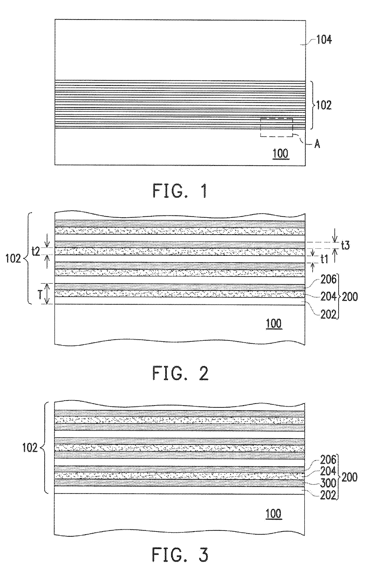
[0023]FIG. 1 is a schematic view of a nitride semiconductor structure according to an embodiment of the invention.
[0024]Referring to FIG. 1, a nitride semiconductor structure of the present embodiment includes a substrate 100, a buffer stack layer 102 and a nitride semiconductor layer 104. The buffer stack layer 102 is located between the substrate 100 and the nitride semiconductor layer 104, and is configured to alleviate a problem of lattice mismatch between the substrate 100 and the nitride semiconductor layer 104. The nitride semiconductor layer 104 is, for example, formed of a plurality of semiconductor layers including a first-type doped semiconductor layer, a second-type doped semiconductor layer, an active layer and so on. A material of the nitride semiconductor laye...
PUM
| Property | Measurement | Unit |
|---|---|---|
| thickness | aaaaa | aaaaa |
| thickness t3 | aaaaa | aaaaa |
| thickness | aaaaa | aaaaa |
Abstract
Description
Claims
Application Information